Simple electronic component design LED experiment

Simple electronic component design LED experiment

Designing a simple electronic component LED experiment requires detailed consideration of many factors, including the working principle of the LED, the required electronic components, circuit design and manufacturing process.

The process is introduced in detail below, but please note that this is a simple LED experimental example designed with electronic components. To learn more, please bookmark and follow our website, or contact us.

You may need to consult more information or guidance to obtain complete understanding and operational details.

All work on the LED project requires the selection and purchase of electronic components according to your needs.

Understand how LEDs work

Soldering electronic components on a circuit board
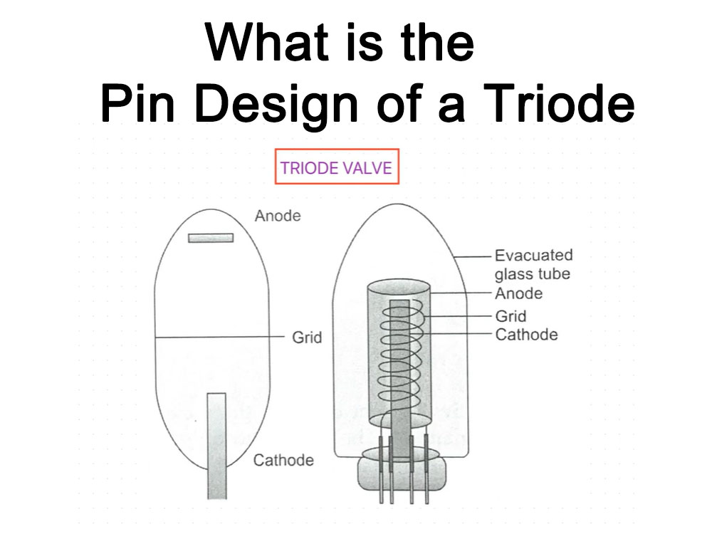
  1. LED (Light Emitting Diode) is a special electronic device that emits light when electric current passes through it. Its working principle is based on the characteristics of the PN junction. When forward biased, current flows from the anode to the cathode, and photons are emitted.
  2. There are many types of LEDs with different colors. Common colors include red, green, blue and other colors. The wavelength of their light is determined by the materials used in the manufacturing process.

Select the required electronic components

Electronic components on a circuit board - LED Circuit Board Assembly Process
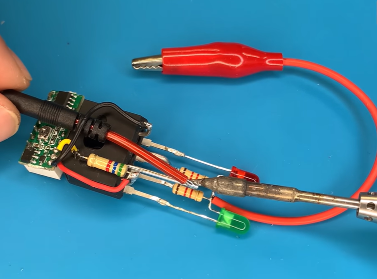
  1. LED: Choose an LED that suits your experimental needs, such as color, size, and brightness.
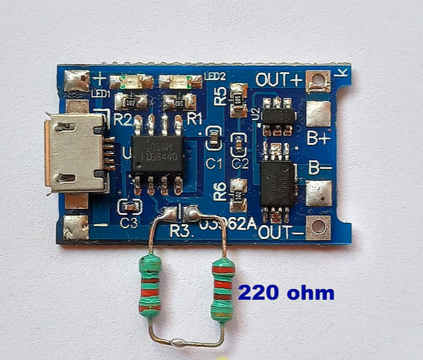
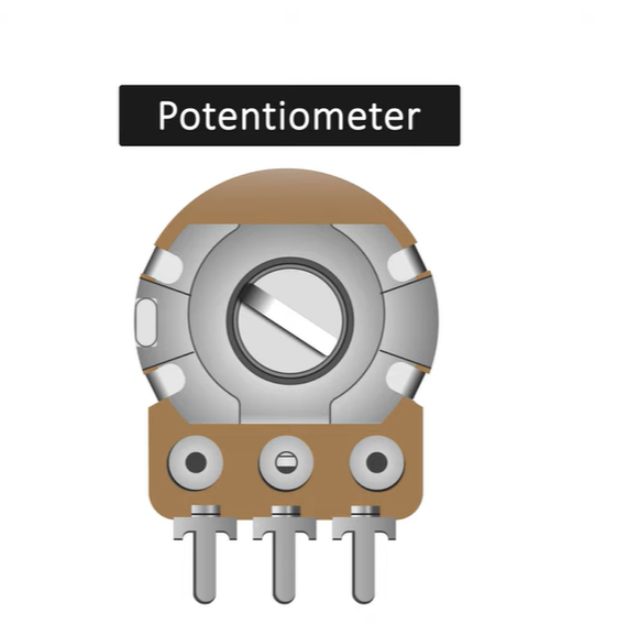
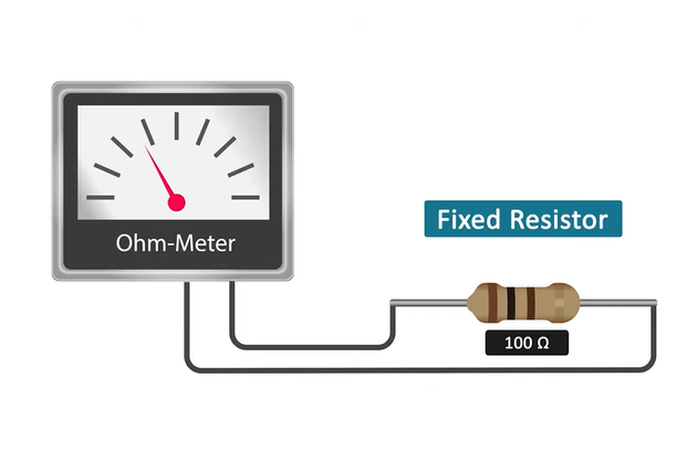
  2. Resistor: used to limit the current flowing through the LED to protect the LED from damage due to excessive current. The formula for calculating the required resistor value is: R = V/I, where R is the resistor value, V is the supply voltage, and I is the current expected to flow through the LED.
  3. Capacitor: used to filter noise in the circuit and protect the LED.
  4. Battery or power supply: Provides power to the LED.
  5. Breadboard: used to build and test circuits.
  6. Wires: used to connect various components.

Design circuit

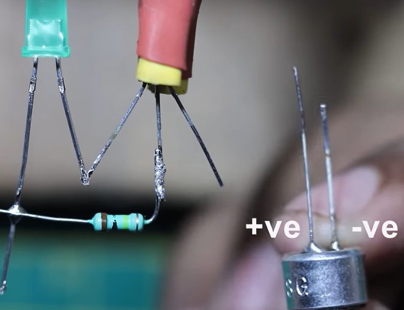
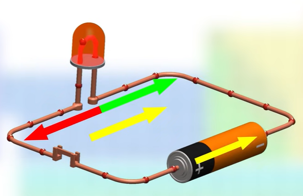
  1. Determine the positive and negative poles of the LED. Generally speaking, the long leg is the positive pole and the short leg is the negative pole.
  2. Design a simple circuit to connect the battery, resistor and LED. Make sure the resistor is connected between the positive terminal of the LED and the battery to limit the current flow.

Build and test circuits

Manual assembly of electronic components on LED board
  1. Place all components on the breadboard and connect them using wires.
  2. Make sure all connections are tight and there is no risk of short circuit.
  3. Add power and observe whether the LED glows. If the LED does not light up, check that the connections are correct and that all components are working properly.
  4. Adjust the brightness of the LED by changing the resistor value or battery voltage.

Further experimentation and exploration

  1. Try using LEDs of different colors to observe their lighting effects under the same conditions.
  2. Use multiple LEDs to design different display modes or patterns.
  3. Connect the LED to the microcontroller and explore ways to program the LED to turn on and off.
  4. Explore using different types of LEDs, such as ultra-bright LEDs or infrared LEDs.
  5. Try connecting the LED to another type of power supply, such as AC power or an adjustable power supply.
  6. Extend the experiment by adding other electronic components, such as using transistors to implement more complex control logic.

Safety Precautions

  1. Always use caution and follow basic safety guidelines when handling circuits and electronic components.
  2. Avoid short circuit or overload during operation to avoid damage to electronic components or risk of fire.
  3. Make sure the power supply voltage matches the rated voltage of the electronic component and avoid using too high or too low voltage.
  4. After the experiment, remember to disconnect the power supply and clean the work area.
  5. If you encounter difficulties or problems, seek professional guidance or consult relevant professionals.

Through this simple electronic component LED experiment, you can gain an in-depth understanding of the working principle of LED, electronic circuit design and basic electronic operation skills. Through continuous experimentation and exploration, you can expand your knowledge and improve your skill level. Remember to always focus on safety issues and follow correct operating procedures and technical requirements.

Understand the relationship between LED brightness and current

The brightness of an LED is directly related to the current flowing through it. By adjusting the resistor value in the circuit, you can change the current flowing through the LED, thereby adjusting the brightness of the LED. This characteristic makes LED a flexible light source that can be used in a variety of different application scenarios.

Understand the lifespan and reliability of LEDs

LEDs generally have longer lifespans because they are less prone to failure under normal operating conditions. However, if the current is too high or the temperature is too high, the LED may be damaged. Therefore, when designing a circuit, you should consider using appropriate protection components, such as resistors and capacitors, to ensure the normal operation of the LED.

Explore different LED applications

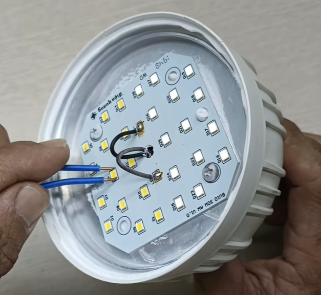
LEDs are used in a wide range of applications, including but not limited to lighting, displays, indicators, backlights, communications, etc. Through this experiment, you can explore the application of LEDs in various scenarios and understand their working principles and design requirements.

Cultivate practical ability and innovative spirit

By designing and building circuits with your own hands, you can develop your practical skills and innovative spirit.

Experiment with different circuit designs and component combinations to explore new applications and solutions. Along the way, you may encounter various problems, but by solving them, you can continue to grow and learn.

In general, through this simple electronic component LED experiment, you can have an in-depth understanding of the working principle, circuit design and electronic operation skills of LED.

At the same time, you can also cultivate your practical ability and innovative spirit, laying a solid foundation for future study and work.

I hope this experiment can stimulate your interest and enthusiasm for electronics and lead you to a broader world of technology.

Frequently Asked Questions

Why do LEDs need series resistors?

Because the characteristic of LED is forward conduction, forward voltage must be applied to both ends of it to light up. Usually the power supply is 5V. If no resistor is added, the current will be very large after being directly connected to the power supply, and it is easy to burn the LED. Adding a resistor can limit the current and protect the LED from being burned.

What is the difference between the anode and cathode of an LED?

The anode of the LED is the positive pole and is connected to the positive pole of the power supply; the cathode is the negative pole and is connected to the negative pole of the power supply. If connected reversely, the LED will not light up and may burn out. Therefore, special attention is required when designing and connecting circuits.

How to choose the appropriate resistor?

Choosing the appropriate resistor depends on the rated voltage and current of the LED. For example, if you are using a 2V, 20mA LED, you can choose a 300 ohm resistor. The calculation formula is: (power supply voltage – LED voltage) / LED current = resistance value.

How to connect LED and resistor?

Connect one end of the LED to the positive terminal of the power supply and the other end to the negative terminal of the power supply through a resistor. Be careful not to connect the positive and negative poles of the LED directly, otherwise the LED will burn out.

How to test whether the LED is working properly?

You can tell whether it is working properly by observing whether the LED lights up. If the LED can light up after forward voltage is applied to both ends, then the LED is normal. If the LED does not light up, you can check whether the circuit is connected normally, or replace the LED with a new one for testing.

What is BD3818KS and specifications datasheet

What is BD3818KS and specifications datasheet

BD3818KS is an audio-specific integrated circuit manufactured by Rohm Semiconductor. It is an 80-BQFP packaged integrated circuit mainly used for audio signal processing.

This integrated circuit has 6 channels, the interface type is serial, the operating voltage range is 5V to 7.4V, and the operating temperature range is -20°C to 75°C.

This integrated circuit is mainly used in consumer audio equipment and has audio signal processing functions.

BD3818KS specifications

Which country is Rohm Semiconductor from?

BD3818KS IC

ROHM Semiconductor Group is a Japanese company founded in 1958 and is one of the most well-known semiconductor manufacturers in the world.

BD3818KS design purpose

BD3818KS and BD3811K1 are 5.1-channel audio processors developed and produced by ROHM, specially designed for home audio and video systems.

BD3811K1 and BD3818KS have built-in mode selectors, input selectors, and have multiple functions, including 6-channel volume, gain amplifier, bass, treble, mix (BD3818KS), dynamic bass boost (BD3818KS) and bass boost (BD3811K1) , these functions are integrated on one chip.

BD3818KS design purpose

BD3818KS Advantages and Disadvantages

Here are the pros and cons of the BD3818KS:

Advantage:

  1. High performance: BD3818KS is a high-performance audio-specific integrated circuit with excellent audio processing capabilities.
  2. High integration: This integrated circuit integrates multiple audio processing functions on one chip, simplifying circuit design and reducing the number of external components.
  3. Easy to use: BD3818KS has a simple and easy-to-use interface to facilitate connection and communication with other devices such as microcontrollers.
  4. High reliability: This integrated circuit has undergone strict quality control and testing and has high reliability.

Disadvantages:

  1. Higher price: BD3818KS is a dedicated audio integrated circuit with a relatively high price, which may increase the cost of the entire system.
  2. Limited scope of application: This integrated circuit is mainly used for consumer audio equipment and may not be suitable for other types of audio equipment.
  3. Lack of flexibility: Since BD3818KS is an application-specific integrated circuit, its functions and performance may be more fixed than general-purpose chips and lack flexibility.

What devices is the BD3818KS suitable for?

BD3818KS is suitable for use on equipment with audio processing requirements, especially for consumer audio equipment.

Since it is an audio-specific integrated circuit, it can play its advantages in devices that require audio signal processing, amplification, sound effect enhancement and other functions. Specifically, devices suitable for using BD3818KS include but are not limited to:

  1. Audio player: used to play music or sounds and perform audio signal processing.
  2. Audio recording equipment: used to record sounds and perform audio signal processing.
  3. Smart speaker: As the core chip for speech recognition and audio output.
  4. Game console: used for audio signal processing and sound effect enhancement.
  5. TV: used for audio signal processing and sound effect enhancement.

It should be noted that the specific scope of application of BD3818KS needs to be determined based on its technical specifications and performance indicators, as well as the overall circuit design and system requirements of the device.

Bd3818ks datasheet manual download (Bd3818ks datasheet pdf)

BD3818KS FAQs

What is BD3818KS?

BD3818KS is an integrated circuit commonly used for audio signal processing. It is produced by Rohm Semiconductor.

What are the main functions of BD3818KS?

BD3818KS is an audio signal processor used to process and optimize audio signals. It can be used in consumer audio equipment to provide clear, high-quality audio output.

What is the operating voltage of BD3818KS?

The operating voltage range of BD3818KS is 5V ~ 7.4V.

What is the packaging form of BD3818KS?

BD3818KS is packaged in 80-BQFP.

What are the application fields of BD3818KS?

BD3818KS is mainly used in consumer audio equipment, such as speakers, headphones, etc., to provide high-quality audio processing capabilities. It can also be used in other areas requiring audio signal processing.

What are the characteristics of BQFP packaging?

The BQFP package has four side pins, and protrusions (cushion pads) are provided at the four corners of the package body to prevent the pins from bending and deforming during transportation. This kind of packaging is suitable for high-frequency lines and is generally installed on PCB boards using SMT technology.

What scenarios is BQFP packaging suitable for?

BQFP packaging is suitable for high pin count, miniaturization and high frequency application scenarios, such as the packaging of highly integrated chips such as microprocessors, digital signal processors (DSP), and FPGAs. In addition, BQFP packaging is also suitable for scenarios that require miniaturization and thinness, such as mobile devices, tablet computers, etc.

What are the advantages of BQFP packaging?

The advantages of BQFP packaging include: small pin spacing and large number of pins, suitable for high-density PCB applications; the package body is thin and lightweight, which is conducive to miniaturization and thinning; using SMT technology, good mounting performance , high reliability.

What are the disadvantages of BQFP packaging?

Disadvantages of BQFP packaging include: due to the long pins, there may be challenges for high-speed signal transmission; compared with BGA packaging, its heat dissipation performance is poor; and the cost is higher.

What is the difference between BQFP packaging and QFP packaging?

The main difference between BQFP packaging and QFP packaging is the setting of the buffer pad. The BQFP package is equipped with protrusions (cushion pads) at the four corners of the package body to prevent the pins from bending and deforming during transportation. The QFP package does not have a buffer pad.

Solar charging control PCB design and component list

Solar charging control PCB design and component list

Hello everyone, my name is AnWen, and today we will share with you the solar charging control PCB design.

In the future, I will share with you DFM manufacturability analysis, PCB design, DFM tools, circuit design and other related knowledge here. Please give me your advice.

What I want to share with you today is: PCB project – MPPT solar charge controller using LT3652. (Attached with project schematic diagram + project information (Gerber) file, please remember to send me a private message to receive it)

Almost every solar-based system has a battery associated with it that must be charged from the sun, and the energy from the battery is used to drive the load. But to use solar panels to charge batteries, a better option is MPPT or maximum power point tracker topology, which has better accuracy than PWM controlled charger.

Working principle of MPPT solar charge controller

MPPT is an algorithm commonly used in solar chargers. The charge controller measures the output voltage of the panel and the battery voltage. By taking these two data, comparing them to determine the optimal power that the panel can provide to charge the battery. .

In any case, whether the sunlight conditions are good or poor, the MPPT charge controller uses this maximum power output factor and converts it into the optimal charging voltage and current for the battery. Whenever the power output of the solar panel decreases, the battery charging current also decreases.

Therefore, in low sunlight conditions, the battery is continuously charged based on the output of the solar panel. This doesn’t usually happen with regular solar chargers. Because every solar panel comes with a maximum output current rating and a short circuit rating.

MPPT is approximately 90%-95% efficient in conversion. Efficiency then also depends on solar driver temperature, battery temperature, solar panel mass and conversion efficiency.

In this project, build a solar MPPT charger for lithium batteries.

Design MPPT Charger

Will charge 2P2S battery (6.4-8.4V)
Charging current is 600mA
There will be an additional charging option using an adapter

List of components required to build the MPPT controller

LT3652 driver
1N5819 – 3 pcs.
10k pot
10uF capacitor – 2 pcs
Green LED
Orange LED
220k resistor
330k resistor
200k resistor
68uH inductor
1uF capacitor
100 uF capacitor – 2 pcs.
Battery – 7.4V
2 1k resistors
Barrel socket

MPPT solar charger circuit diagram

The complete solar charge controller circuit is shown below:

This circuit uses the LT3652, a complete monolithic step-down battery charger that operates from an input voltage range of 4.95V to 32V. Therefore, the maximum input range for solar and adapter is 4.95V to 32V.

The LT3652 provides a constant current/constant voltage charging feature that can be programmed through a current sense resistor for a maximum charge current of 2A.

Output Section: The charger uses a 3.3V float voltage feedback reference so any desired battery float voltage up to 14.4V can be programmed using a resistor divider.

The LT3652 also contains a programmable safety timer using a simple capacitor, which is used to terminate charging after a desired time, useful for detecting battery failure.

The LT3652 requires MPPT setting, and one of the potentiometers can be used to set the MPPT point. When the LT3652 is powered by a solar panel, the input regulation loop is used to maintain the panel at peak output power. How to maintain regulation depends on the MPPT setting potentiometer.

MPPT solar charger value setting

  1. Battery voltage setting
    VR1 is used to set the MPPT point, R2, R3, and R4 are used to set the 2S battery charging voltage (8.4V). The formula for setting the battery voltage is as follows:

RFB1 = (VBAT(FLT) • 2.5 • 10 5 )/3.3

RFB2 = (RFB1 • (2.5 • 10 5 ))/(RFB1 – (2.5 • 10 5 )) (set battery voltage formula)

  1. Timer settings
    Capacitor C2 is used to set the charging timer, which can be set using the following formula:

tEOC = CTIMER • 4.4 • 10 6 (in hours) (set timer)

D3 and C3 are the boost diode and boost capacitor that drive the internal switch and promote saturation of the switching transistor. The boost pin operates from 0V to 8.5V.

  1. Charging current setting
    R5 and R6 are parallel current sensing resistors, and the charging current can be calculated using the following formula:

RSENSE = 0.1/ICHG(MAX) (set charging current)

The current sense resistors in the schematic are chosen to be 0.5 Ω and 0.22 Ω, which are combined in parallel to produce 0.15 Ω. Using the above formula it will produce a charging current of almost 0.66A, C4, C5 and C6 are the output filter capacitors.

How the DC barrel jack is connected: If you plug the adapter jack into the adapter socket, the solar panel will disconnect. D1 will protect the solar panel or adapter from reverse current flow during no charging conditions.

Solar Charge Controller PCB Design

For the MMPT circuit discussed above, the MPPT charger controller 3D PCB diagram is designed, as shown below:

Solar Charge Controller PCB Design

The design has a GND copper plane with appropriate connecting vias, the LT3652 requires an adequate PCB heatsink, which is created using a GND copper plane and placing the vias in the solder plane.

Solar charger PCB board electronic component assembly
Testing the MPPT Solar Charger

Assembling the MPPT Solar Charge Controller

The physical picture of the MPPT charger controller PCB is shown below:

Assembling the MPPT Solar Charge Controller - MPPT charger controller PCB physical picture

Testing the MPPT Solar Charger

To test the circuit, a solar panel rated 18V .56A was used. The picture below is the detailed specifications of the solar panel.

Testing the MPPT Solar Charger

Detailed specifications of solar panels

How to test solar charger PCB board

The complete circuit was tested under mild sunlight conditions using a 2P2S battery (8.4V 4000mAH) battery for charging –

After everything is connected, set the MPPT when the sun conditions are right and control the potentiometer until the charging LED starts glowing and the circuit is working smoothly.

Frequently Asked Questions

What issues need to be paid attention to when designing solar charging control PCB?

Issues that need attention in solar charging control PCB design include power management, current and voltage stability, charging protection, safety performance, energy efficiency ratio, component layout and wiring, etc.

How to ensure the stability and reliability of solar charging control PCB design?

To ensure the stability and reliability of solar charging control PCB design, it is necessary to select appropriate components, conduct sufficient testing and verification, and use technical means such as multi-layer PCB board design to improve the electrical and mechanical properties of the PCB board.

What issues need to be paid attention to in component layout and wiring in solar charging control PCB design?

In terms of component layout and wiring, it is necessary to consider the arrangement order of components, heat dissipation performance, electromagnetic interference and other factors, and rationally plan component layout and wiring to reduce electromagnetic interference and improve heat dissipation performance.

What issues need to be paid attention to in terms of safety performance in solar charging control PCB design?

In terms of safety performance, it is necessary to consider issues such as overload protection, short-circuit protection, temperature protection, etc., and take corresponding protective measures to ensure the safety and stability of the circuit.

How to evaluate the energy efficiency ratio of solar charging control PCB design?

Energy efficiency ratio is one of the important indicators for evaluating solar charging control PCB design. It can be evaluated through experimental testing and simulation analysis to improve the overall performance of the solar charging control system.

How to choose suitable components to design solar charging control PCB?

Choosing suitable components is one of the keys to designing solar charging control PCB. It is necessary to consider the performance parameters, reliability, cost and other factors of the components to select components with stable quality and reliable performance.

What is a solar charging control panel?

Solar charging control panel is an electronic device used in solar photovoltaic systems to control the charging and discharging process. Its main function is to convert the electric energy generated by the solar panel into direct current, and charge the battery through the control circuit, while preventing overcharging and protecting the battery.

What are the main components of a solar charging control panel?

Common components of solar charging control panels include solar panels, batteries, charging control circuits, discharge control circuits and protection circuits. Among them, the charge control circuit and the discharge control circuit are the core components, used to realize automatic charge and discharge control and extend battery life.

How does a solar charging control panel work?

The working principle of the solar charging control panel is to use the photovoltaic effect principle to convert solar energy into electrical energy, and charge the battery through the charging control circuit. When the sun shines on the solar panel, the panel will generate direct current. The charging control circuit will adjust the charging current through PWM (pulse width modulation) according to the battery’s power and charging status to achieve automatic charge and discharge control. At the same time, the protection circuit can prevent the battery from overcharging and over-discharging to extend the service life of the battery.

How to choose the right solar charging control panel?

When choosing a suitable solar charging control panel, you need to consider the following aspects:
Voltage and current requirements: Select the appropriate control board according to the voltage and current requirements of the load to ensure sufficient power supply.
Power requirements: Select an appropriate control board according to the power requirements of the load to ensure sufficient power output.
Charging method: Choose the appropriate charging method according to the actual situation, such as PWM constant current charging, PWM constant voltage charging, etc.
Protection function: Choose a control board with overcharge, over-discharge, over-current, short-circuit and other protection functions to ensure the safe and stable operation of the system.
Installation environment: Consider the impact of the installation environment on the control panel, such as temperature, humidity, sun protection, etc., and select a control panel with suitable environmental conditions.

What is the pin design of a triode

What is the pin design of a triode

A triode is an electronic component made on a semiconductor substrate. It consists of two PN junctions that are very close to each other.

These three parts divide the entire semiconductor into three parts: base area, emitter area and collector area.

Depending on the arrangement of the semiconductor materials, there are two types of transistors: PNP and NPN.

Transistor pin design

The pin design of the triode means that the triode has three pins, which are the base (Base, referred to as B), the collector (Collector, referred to as C) and the emitter (Emitter, referred to as E).

Transistor pin design core

These three pins correspond to the three areas inside the triode, and each pin has its specific function and role.

Base (B):

The base is the control electrode of the triode. It controls the amplification of the triode by controlling the input of current. Small changes in the base current will cause large changes in the collector current, thereby achieving current amplification.

Collector (C):

The collector is the main output terminal of the triode. It is responsible for collecting and outputting the amplified current. When the triode is working, a certain voltage needs to be applied between the collector and the emitter to maintain the normal operation of the triode.

Emitter (E):

The emitter is another important output terminal of the triode. It forms a PN junction together with the base and collector to achieve current amplification. The current change of the emitter is controlled by the base current. When the base current increases, the emitter current will also increase accordingly.

In the actual application of triodes, the pin design allows the triode to be easily connected and combined with other electronic components to achieve various complex circuit functions.

Transistor pin design core

For example, in the microcontroller application circuit, the triode mainly plays the role of a switch, controlling the on-off of the entire circuit by controlling the on-off of the base current. In addition, triodes can also be used for circuit functions such as signal amplification and modulation.

Why do we need to design the pins of the triode?

The pins of the transistor are designed for efficient connection and utilization. First of all, through reasonable pin design, reliable connection between the triode and other electronic components can be achieved to ensure the stability and reliability of the circuit. Secondly, the pin design can optimize the input and output of current and signals, thereby optimizing the working efficiency and performance of the triode. In addition, reasonable pin design can also facilitate the detection, repair and replacement of triodes, improving the maintainability and reliability of electronic equipment. In short, the pins of the triode are designed to meet various needs in practical applications and to achieve efficient, stable and reliable operation of electronic equipment.

Pin welding process

How are the pins of the triode designed?

The transistor is a common electronic component with three electrodes, namely base b, collector c and emitter e.

In terms of pin design of transistors, certain standards are generally followed to ensure compatibility with other components and circuits.

Here are some key points about transistor pin design:

  1. Pin arrangement: The pin arrangement sequence of triodes is usually determined according to international standards. Normally, the three pins of a triode are arranged in a certain order, usually in the order of base, collector and emitter. In circuit diagrams, they are also labeled and annotated in this order.
  2. Pin function: The function of each pin is specific. The base is the control electrode, the collector is the input electrode, and the emitter is the output electrode. In the circuit, by controlling the size of the base current, the current flow between the collector and the emitter can be controlled, thereby achieving functions such as signal amplification and switching control.
  3. Package type: There are many package types of transistors, and each package type has different pin arrangements and sizes. For example, TO-92 packaging, TO-220 packaging, SOT-23 packaging, etc. When designing these package types, factors such as pin arrangement, pin spacing, and pin length need to be considered to ensure that the components can be successfully installed on the circuit board.
  4. Pin spacing: Pin spacing refers to the distance between two adjacent pins. The size of this distance has a certain impact on the installation of components and the layout of the circuit board. Generally speaking, the larger the pin spacing, the easier it is to install and solder components, and it will also help improve the anti-interference performance of the circuit board.
  5. Lead length: Lead length is the length from the bottom of the component to the top of the lead. When selecting the pin length, two factors need to be considered: one is the convenience during soldering, and the other is the space for the circuit board layout. If the pin length is too long, it may cause problems such as instability during soldering or short circuits with other components; if the pin length is too short, it may affect the layout and routing of the circuit board.

When designing the transistor pins, you also need to pay attention to the following points:

  1. Consider package type and size: Different package types have different sizes and pin arrangements. You need to choose the appropriate package type and size according to actual needs.
  2. Consider circuit board layout and wiring: When selecting pin length and spacing, you need to consider the needs of circuit board layout and wiring to ensure the stability of component installation and the reliability of circuit performance.
  3. Follow standards: When designing pins, international standards and industry specifications should be followed to ensure that the designed transistor is compatible with other components and circuits.
  4. Conduct simulation and testing: During the design process, simulation and testing can be performed to verify the feasibility and reliability of the design. This helps reduce errors and defects in the design and improves the success rate of the design.

In short, transistor pin design is a process that requires consideration of multiple factors. In the design, multiple aspects such as package type, functional requirements, circuit board layout, and standard specifications should be comprehensively considered.

Through reasonable design, the stability and reliability of the triode in the circuit can be ensured, thereby improving the performance and quality of the entire circuit.

Design rules for transistors and transistors in circuits

International standards

There is no unified international standard for transistor pin design, because different manufacturers and different application scenarios may use different pin arrangement sequences. However, there are some common pin ordering and labeling methods to facilitate user understanding and use.

A common pin arrangement is the TO-92 packaged triode, whose pin arrangement is base, collector, and emitter. On the pins of the TO-92 package, the numbers 1, 2, and 3 are usually marked, corresponding to the base, collector, and emitter respectively. In addition, the letters B, C, and E are also marked on the pins of some triodes, which represent the base, collector, and emitter respectively.

Another common pin arrangement is the SOT-23 packaged transistor, whose pin arrangement is emitter, base, collector. On the pins of the SOT-23 package, the numbers 1, 2, and 3 are usually marked, corresponding to the emitter, base, and collector respectively. In addition, the letters E, B, and C are also marked on the pins of some triodes, which represent the emitter, base, and collector respectively.

In addition to the common pin arrangement order and labeling methods, there are also some special transistors that may use non-standard pin arrangement order and labeling methods. Therefore, when selecting and using a triode, users need to carefully check the triode’s specification sheet or circuit diagram to ensure correct connection and use.

It should be noted that the pin arrangement of transistors from different manufacturers may be different. Therefore, in actual use, it is necessary to carefully check the pin arrangement and labeling of the transistors to avoid connection errors that may cause abnormal circuit operation. At the same time, for some special application scenarios and specially packaged transistors, users need to select and use them according to specific requirements.

Transistor pin design FAQs

What is the main function of a triode?

The main function of the triode is current amplification.

Why can’t the emitter and collector of a triode be interchanged at will?

The manufacturing process of the emitter and collector of the triode is not symmetrical, and its structure is not symmetrical. If replaced, the amplification capacity will be much smaller than before replacement, and the pressure resistance will also be much smaller.

Under the operating conditions of the amplification region, what is the bias state of the transistor collector?

When working in the amplification zone, the collector is in a reverse biased state. At this time, if the base lead is disconnected and U_{CE} is large during operation, the collector junction may be broken down due to excessive reverse voltage.

How many regions are the input and output characteristic curves of a triode divided into?

Generally divided into amplification area, saturation area and cut-off area.

What are the basic configurations of amplifier circuits?

There are three basic configurations of amplifier circuits, namely common emitter, common base and common collector.

What are the bias circuits in a common emitter amplifier circuit?

In the common emitter amplifier circuit, there are three types of bias circuits: upper base bias, voltage divider type and set-base feedback type.

In what area of the triode input-output characteristic curve should the amplifier’s quiescent operating point lie?

It should usually be in the center of the amplification area of the triode’s input-output characteristic curve.

What does the determination of the static operating point mean for the amplifier?

Correctly determining the static operating point enables the amplifier to have minimum cutoff distortion and saturation distortion, while also obtaining the maximum dynamic range and improving the efficiency of the triode.

What material is the triode emitter made of?


The emitter of a transistor is usually made of N-type silicon material, that is, the silicon material is doped with a small amount of pentavalent elements, such as phosphorus (P) or arsenic (As). These materials have an excess of free electrons and therefore have high electrical conductivity.
However, in actual applications, other materials may be used to make the emitter depending on the specific purpose and performance requirements of the triode. For example, in some high-frequency applications, materials such as gallium arsenide (GaAs) or indium phosphide (InP) may be used to make the emitter. These materials have higher carrier mobility and shorter carrier lifetime, providing higher emission efficiency and frequency response.

What material is the base of a triode made of?

The base material of the triode is usually silicon (Si). Silicon is a common semiconductor material with good electrical conductivity and thermal stability. Silicon material has a high energy band width, which allows it to operate at room temperature and is suitable for most electronic devices. Silicon materials also have high electron mobility and low electron affinity, allowing triodes to achieve high-frequency amplification and switching operations.

What material is the triode collector made of?

The collector of a transistor is usually made of N-type silicon material, that is, the silicon material is doped with a small amount of pentavalent elements, such as phosphorus (P) or arsenic (As). N-type silicon materials have excess free electrons and therefore have higher conductivity.

What is SOT-23 package

What is SOT-23 package

The SOT-23 package is a small surface mount package commonly used in integrated circuits (ICs) and semiconductor devices.

Generally, small-profile transistors with less than or equal to 5 pins.

SOT-23 stands for “Small Outline Transistor 23”. This package is widely used in many electronic devices due to its compact size, good heat dissipation performance and adaptability.

The SOT-23 package is a three-pin surface mount package commonly used for integrated circuits, diodes, transistors and other components.

Definition

It is divided into two types according to the surface width, one with a width of 1.3mm and the other with a width of 1.6mm. The corresponding Socket models are 4330 121 and 4331 121 respectively. Need to pay attention when using it.

Width category:

1.3mm, 1.6mm

Socket model:

4330 121 (corresponds to 1.3mm), 4331 121 (corresponds to 1.6mm)

Advantage

The advantages of SOT-23 packaging include the following aspects:

  1. Miniaturization: The SOT-23 package has a compact size to meet the growing demand for miniaturized electronic products.
  2. High reliability: Due to its sturdy and compact design, the SOT-23 package can effectively protect the internal components from the external environment, thus improving its reliability.
  3. Easy to solder: SOT-23 package has good soldering performance, which can ensure reliable connection between components and circuit boards.
  4. Reduce costs: Due to its miniaturization and high reliability, SOT-23 packaging can help manufacturers reduce production costs and improve production efficiency.
  5. High performance: SOT-23 package can provide good electrical and thermal performance to support high-performance electronic applications.
SOT-23 transistor

In short, the SOT-23 package has the advantages of miniaturization, high reliability, easy welding, cost reduction, and high performance, so it is widely used in many electronic devices and products.

Disadvantage

The SOT-23 package also has some disadvantages in some aspects. First, due to its compact size, the SOT-23 package may not be suitable for applications requiring high power or high current. Secondly, because the components in its package are very dense, the heat dissipation performance may be limited, and special attention needs to be paid to thermal management issues. In addition, due to the higher price of the SOT-23 package, it may not be suitable for some cost-sensitive applications.

In summary, although the SOT-23 package has many advantages, you need to pay attention to its potential shortcomings when using it, and take appropriate measures to overcome these problems.

Classic application cases of SOT-23 packaging

The following are some application examples of SOT-23 in life. SOT is generally a small outline transistor with less than or equal to 5 pins.

sot-23 dimensions

Look at the picture, this is the SOT-23 package shape

SOT-23 is divided into two types according to the surface width, one is 1.3mm wide and the other is 1.6mm wide. The corresponding Socket models are 4330 121 and 4331 121 respectively. Need to pay attention when using it.

Mobile devices

SOT-23 packaged components are commonly used in mobile devices such as smartphones, tablets, and digital cameras. For example, power management chips, battery management chips, amplifiers, sensors, etc. can all be packaged in SOT-23.

Household electronic products

SOT-23 is commonly used in control circuits and signal processing circuits in household electronic products. For example, power management chips, amplifiers, filters and other components in televisions, audio equipment, wireless routers and other products may be packaged in SOT-23.

Automotive electronics

SOT-23 is also widely used in automotive electronic systems. For example, sensors, drivers, switches, etc. in the engine control unit (ECU) are often packaged in SOT-23. In addition, some auxiliary chips in vehicle entertainment systems, navigation systems, etc. may also be packaged in SOT-23.

Smart Home

SOT-23 packaged components can be used in control and sensing circuits in smart home devices. For example, microcontrollers, wireless communication chips, sensors, etc. in smart light bulbs, smart sockets, smart door locks and other products often use SOT-23 packaging.

Medical equipment

SOT-23 packaging also has certain applications in medical equipment. For example, control circuits, signal processing circuits, etc. in medical instruments can be packaged in SOT-23.

sot-23 size specifications

It should be noted that the specific applications of SOT-23 packaging in various fields may vary depending on product design and requirements. The above are just some common examples, and actual application scenarios may be more extensive and diverse.

SOT-23 packaging FAQs

What is the SOT-23 package?

The SOT-23 package is a small surface mount package commonly used in integrated circuits (ICs) and semiconductor devices.

What are the advantages of SOT-23 packaging?

The advantages of SOT-23 packaging include miniaturization, high reliability, easy soldering, cost reduction and high performance.

What is the pinout sequence for SOT-23 packages?

The pin arrangement of the SOT-23 package is usually emitter, base, and collector.

What are the application scenarios of SOT-23 packaging?

SOT-23 packaging is widely used in various electronic equipment, such as computers, communication equipment, consumer electronics, etc.

How to identify the pinout sequence of a SOT-23 package?

You can usually see numerical labels on the pins of the SOT-23 package. For example, labels 1, 2, and 3 correspond to the emitter, base, and collector respectively.

Why use SOT-23 package?

The use of SOT-23 packaging can meet the growing demand for miniaturized electronic products, while its compact size, good thermal performance and adaptability also make it a reliable choice.

What are the common component types in SOT-23 packages?

SOT-23 packaging is commonly used for integrated circuits, diodes, transistors and other components.

What are the characteristics of SOT23 package?

The SOT23 package has the advantages of small PCB footprint, discrete and easy layout, independent functions, wide selection range, and low price, and is favored by hardware engineers.

What is the pinout of the SOT23 package?

The SOT23 package usually has 3 pins, namely base (B), emitter (E) and collector (C). The specific order of pin distribution depends on the specific device type, but usually follows certain rules. For NPN transistors, the pin sequence is BEC or CBE; for PNP transistors, the pin sequence is CBE or BEC.

How to quickly identify SOT23 packaged components?

In the absence of a schematic, components can be identified by observing the silk screen or model identification on the SOT23 package. In addition, you can get more information by looking for relevant component information or specifications provided by the manufacturer.

What are the common device types in SOT23 packages?

SOT23 packaging is commonly used to package transistors, MOS tubes, transient suppression diodes (TVS) and other devices. Different device types have different internal structures and circuit functions, so it is necessary to select the appropriate device type according to the specific situation when using it.

How to correctly use SOT23 packaged devices?

When using SOT23 packaged devices, you need to follow the correct circuit connection method and parameter matching principles. At the same time, it is necessary to pay attention to the extreme parameters and usage conditions of the device to avoid damage or unstable performance caused by excessive use.
When installing and welding, you also need to pay attention to following the correct process requirements to avoid problems such as virtual welding and short circuits.

What are precision electronic components

What are precision electronic components

Precision components refer to electronic components with high precision, good stability, and high reliability. They are usually used in circuits, systems, and instruments that require high precision.

Compared with ordinary components, precision components require higher precision and better stability, and can maintain relatively stable electrical parameters and mechanical properties in the working environment.

Resistors, capacitors, inductors, transistors, and integrated circuit precision electronic components form a PCB board circuit

Common precision components include resistors, capacitors, inductors, transistors, integrated circuits, etc. These components have the characteristics of simple structure, clear principle, reliable performance and long service life.

The meaning of precision electronics

It refers to electronic products or components that are manufactured with very high precision and very small errors. In the machinery and electronics industries, the word precision is usually used to describe products or components that require extremely high precision, complex manufacturing processes, and require the use of advanced production equipment and testing methods to ensure product quality and stability.

Precision Electronic Components KU Series Panel Mount Potentiometers

Main feature

The main characteristics of precision electronic components include high precision, high reliability, high stability, high consistency, low noise and low power consumption.

Precision Electronic Components

Types of precision electronic components

There are many types of precision electronic components, which can be roughly divided into the following categories according to their functions and uses:

  1. Resistor: A resistor is a device used to control electrical transmission, mainly used to control current, voltage and power. According to different materials, they can be divided into carbon film resistors, metal film resistors, thermistors, etc. Among them, carbon film resistors have the characteristics of high precision and good stability, and are often used in precision measurement, circuit calibration and other fields.
  2. Capacitor: A capacitor is a device used to store and release charges. It is mainly used to regulate voltage and current. It can be divided into ceramic capacitors, dielectric capacitors, ohmic capacitors, etc. according to materials. Among them, ceramic capacitors have the characteristics of fast frequency response and electrical stability, and are usually used in high-precision circuits such as electronic computers and navigation systems.
  3. Inductor: An inductor is a component that can store magnetic field energy and is mainly used in circuits such as filtering, oscillation, and voltage transformation. Precision inductors have the characteristics of high precision, high Q value, and low loss, and are widely used in communications, radar, medical electronics and other fields.
  4. Diodes and transistors: Diodes and transistors are semiconductor devices with functions such as amplification, switching, and voltage stabilization. Precision diodes and transistors have the characteristics of low power consumption, high speed, and high reliability, and are widely used in integrated circuits, power electronics and other fields.
  5. Sensor: A sensor is a device that can convert physical quantities into electrical signals, such as pressure sensors, temperature sensors, photoelectric sensors, etc. Precision sensors have the characteristics of high precision, high sensitivity, and high stability, and are widely used in automation, robotics, aerospace and other fields.

In addition to the above types of components, there are many other types of precision electronic components, such as filters, oscillators, crystal oscillators, field effect transistors, etc. These components play an important role in their respective fields and provide a solid foundation for the development of modern electronic technology.

How to Make Precision Electronic Components

Manufacturing precision electronic components requires the use of a series of advanced processes and technologies, including microelectronics manufacturing technology, precision processing technology, thin film deposition technology, photolithography and etching technology, etc. These technologies can produce high-precision and high-stability electronic components at the nanometer level to meet various complex and precise application requirements.

Precision electronic components on PCB boards include resistors, capacitors, inductors, transistors, integrated circuits, etc.

Specifically, microelectronics manufacturing technology is a manufacturing technology that integrates microelectronic devices, circuits and systems on a chip. It includes integrated circuit manufacturing, micro-nano device manufacturing, thin film manufacturing and other aspects, and is one of the core technologies for manufacturing precision electronic components.

Precision machining technology is a technology for manufacturing mechanical components and structures with high precision, high surface quality, and high stability. It includes micro-cutting, grinding, grinding, polishing and other processes, which can process very fine and complex mechanical parts.

Thin film deposition technology is a technology that deposits thin film materials on the surface of a substrate. It includes physical vapor deposition, chemical vapor deposition and other methods, which can prepare thin film materials with high purity, high density and high adhesion. It is one of the important processes for manufacturing precision electronic components.

Photolithography and etching technologies are key technologies for manufacturing integrated circuits and micro-nano devices. Photolithography is to irradiate the designed circuit pattern onto the photosensitive material through a light beam to cause a chemical reaction to form a copy of the circuit pattern; etching is to use the copied circuit pattern to change the circuit pattern from the chemical reaction or physical impact. The base material is peeled off to form the actual circuit.

In addition to the above technologies, manufacturing precision electronic components also requires the use of a series of auxiliary processes and technologies, such as electroplating, coating, heat treatment, etc. These processes and technologies can improve the electrical performance, mechanical performance and environmental adaptability of components, thereby improving the reliability and stability of components.

In short, manufacturing precision electronic components requires the use of a series of high-precision processes and technologies, which requires a high degree of specialization and technology accumulation. At the same time, it is also necessary to continuously introduce new technologies and develop new products to meet the growing market demand.

Manufacturing Equipment

Precision electronic component manufacturing equipment mainly includes the following categories:

  1. Manufacturing equipment: such as printing machines, placement machines, welding machines, cutting machines, etc., used to manufacture and assemble electronic components. These devices require high precision and stability to ensure that the electronic components manufactured meet the requirements.
  2. Testing equipment: such as testing machines, microscopes, oscilloscopes, etc., used to test the performance and quality of electronic components. These devices require high precision and sensitivity to ensure the accuracy and reliability of detection results.
  3. Auxiliary equipment: such as cleaning machines, dryers, coating machines, etc., used to assist in the manufacturing and testing of electronic components. These devices require high precision and efficiency to ensure the quality and production efficiency of electronic components.

These equipment need to have high precision, high stability, high reliability and other characteristics to meet the manufacturing and testing requirements of precision electronic components.

In addition, with the continuous advancement of technology and increasing application requirements, manufacturing equipment is also constantly developing and innovating to adapt to new manufacturing processes and higher performance requirements.

Application areas

  1. Communication field: Precision electronic components are used to manufacture communication equipment, optical communication devices, mobile communication base stations, etc., supporting high-speed data transmission and signal processing.
  2. Automotive electronics field: Precision electronic components are used in automobile control systems, sensors, actuators, etc. to improve the safety, comfort and fuel economy of automobiles.
  3. Computer and network fields: Precision electronic components are indispensable components for manufacturing computer processors, memory modules, network equipment, etc., supporting the computing and data transmission of computers and networks.
  4. Digital audio and video field: Precision electronic components are used in high-definition video processing, audio processing, etc. to provide high-quality audio-visual experience.
  5. Aerospace field: Because precision electronic components have the characteristics of high stability and high reliability, they are used to manufacture aerospace equipment, satellite communications, etc.
  6. Medical electronics field: Precision electronic components are used in medical equipment, such as medical imaging equipment, surgical robots, etc., to improve the level and efficiency of medical services.

These application fields have very high requirements on the performance and quality of precision electronic components, so advanced manufacturing processes and technologies are required to ensure their quality and stability.

At the same time, with the continuous advancement of technology and increasing application requirements, precision electronic components are also constantly developing and innovating to meet the stringent requirements of various fields.

Frequently Asked Questions

What are precision electronic components?

Precision electronic components refer to those electronic products or components that are manufactured with very high precision and with very small errors. They have the characteristics of high precision, high stability, and high reliability, and are widely used in various fields that require high performance of electronic components.

What types of precision electronic components are there?

There are many types of precision electronic components, including resistors, capacitors, inductors, diodes, transistors, sensors, etc. These components play an important role in their respective fields and provide support for the development of modern electronic technology.

What is the difference between precision electronic components and ordinary electronic components?

The main difference between precision electronic components and ordinary electronic components is their accuracy and stability. Precision electronic components are manufactured with higher precision, smaller error ranges, and can work stably under more stringent conditions. In addition, the materials and processes of precision electronic components are also more advanced and sophisticated.

Why do we need to use precision electronic components?

Precision electronic components can provide higher circuit performance and more reliable working performance to meet the needs of various complex and precise applications. In many fields, such as communications, medical electronics, aerospace, etc., the performance requirements of electronic components are very high. Precision electronic components must be used to ensure the normal operation and performance of the equipment.

How to choose suitable precision electronic components?

Selecting appropriate precision electronic components requires consideration of multiple factors, including component specifications, performance parameters, accuracy levels, working environment, etc. In addition, it is necessary to select appropriate component types and brands according to specific application requirements, and conduct reasonable circuit design and component layout.

How to ensure the quality and stability of precision electronic components?

Ensuring the quality and stability of precision electronic components requires the use of advanced manufacturing processes and technologies, as well as strict quality control and testing. In addition, you also need to pay attention to the storage and use environment of components to avoid being affected by adverse factors such as temperature, humidity, and static electricity.

What is an ultrasonic generator?

What is an ultrasonic generator

Ultrasonic generator, also known as ultrasonic drive power supply, electrical box, and controller, is an important component of high-power ultrasonic system.

The high-frequency AC signal matched by the ultrasonic generator and the ultrasonic transducer is used to drive the ultrasonic transducer to work.

What is the function of ultrasonic generator

The function of the ultrasonic generator is to convert the mains power into a high-frequency AC signal that matches the ultrasonic transducer and drive the ultrasonic transducer to operate.

High-power ultrasonic power supplies generally use switching power supply circuits in terms of conversion power.

Ultrasonic power supplies are divided into self-excited and other-excited power supplies. The self-excited power supply is called ultrasonic simulation power supply, and the other-excited power supply is called ultrasonic generator.

Working principle of ultrasonic generator

ultrasonic generator introduction (industrial grade)

An ultrasonic generator, also known as an ultrasonic power supply or ultrasonic transducer, is a device that converts electrical energy into mechanical energy. It uses the principle of the piezoelectric effect to drive the piezoelectric ceramic material by applying high-frequency AC voltage, causing it to produce mechanical vibrations of the same frequency.

The working principle of the ultrasonic generator can be summarized as follows:

  1. AC voltage: Ultrasonic generators usually use 220V or 380V AC voltage as input, and convert it into DC voltage through rectification and filtering.
  2. Oscillator: The oscillator is the core part of the ultrasonic generator. It can be a self-excited oscillator or a self-excited oscillator. The self-excited oscillator generates oscillation through a positive feedback circuit, while the self-excited oscillator requires an external signal source to provide an excitation signal.
  3. Piezoelectric ceramics: Ultrasonic generators use the piezoelectric effect of piezoelectric ceramics to convert electrical energy into mechanical energy. When piezoelectric ceramics are acted upon by an external electric field, they deform and produce mechanical vibrations.
  4. Resonance unit: In order for the ultrasonic generator to work properly, it needs to match the impedance and frequency of the ultrasonic resonance unit. The resonant unit usually consists of an adjustable capacitor and a fixed impedance resistor to adjust the resonant frequency and impedance matching.
  5. Amplifier: Since the amplitude of the transducer output is low, usually only a dozen microns, an amplifier is needed to amplify the amplitude. The amplifier amplifies the mechanical vibration signal output by the transducer so that it has sufficient energy for various applications.

In short, an ultrasonic generator is a device that uses the piezoelectric effect to convert electrical energy into mechanical energy.

Ultrasonic generator module

Its working principle is to drive the piezoelectric ceramic material by applying high-frequency AC voltage to produce mechanical vibration at the same frequency, and adjust the parameters of the output signal through the resonant unit and amplifier.

What are the types of ultrasonic generators?

There are many types of ultrasonic generators, which can be divided into the following types according to different classification methods:

  1. According to the working frequency, it can be divided into low frequency (100hz) and medium frequency (100~10mhz) ultrasonic generators.
  2. According to the energy conversion mode, it can be divided into electromagnetic, piezoelectric ceramic and semiconductor ultrasonic generators.
  3. According to the output waveform, it can be divided into continuous wave and pulse wave ultrasonic generators.
  4. According to power, it can be divided into small power, medium power and high power ultrasonic generator.
  5. According to the circuit structure, it can be divided into self-excited and separately excited ultrasonic generators.

In addition, there are some specific classifications, such as frequency-adjustable ultrasonic generators, 100W/300W ultrasonic generators, low-power ultrasonic generators, high-frequency ultrasonic generators, large-function ultrasonic generators, and digital display ultrasonic generators according to function. Generator etc.

How to judge the quality of ultrasonic generator

The quality of ultrasonic generators is generally judged from the following two points:

  1. Check whether the output power is constant. We know that when the voltage of the ultrasonic power supply changes. The output power of the ultrasonic power supply will also change. At this time, the mechanical vibration reflected on the ultrasonic transducer will become larger and smaller, causing the cleaning effect to be unstable. Therefore, it is necessary to stabilize the output power and adjust the power amplifier accordingly through the power feedback signal to make the power amplification stable.
  2. Check whether frequency tracking is efficient. When the ultrasonic transducer works at the resonant frequency point, it has the highest efficiency and the most stable operation. However, the resonant frequency point of the ultrasonic transducer will change due to assembly reasons and aging of the work. Of course, this change is only a frequency drift and does not change. It will be huge. Frequency tracking can control the frequency of the ultrasonic generator to follow the resonant frequency point of the ultrasonic transducer within a certain range. Let the generator always work at its best.

Matching problem between ultrasonic generator and transducer

Among ultrasonic cleaning machines of the same model, if the ultrasonic generator and transducer are well matched and debugged, the cleaning effect will be better; if the ultrasonic generator and transducer are poorly matched and debugged, the cleaning effect will be poor.

For the same ultrasonic system, if the cleaning effect deteriorates after working for a period of time, or the vibration box is replaced, the impedance matching circuit needs to be re-adjusted.

Different from the matching of general electronic equipment, the impedance matching of ultrasonic generators not only solves the problem of rheostat, but also solves the problem of tuning.

At present, most companies conduct matching and debugging based on the personal experience of ultrasonic engineers, and the matching effect also depends on people. different.

In actual application scenarios, some manufacturers found that the ultrasonic wave debugged in the factory was not effective at the customer’s end.

There are also customers asking why their cleaning equipment is running normally, but the cleaning quality of the products is unstable. There are many factors involved, and the failure of the ultrasonic system to match well is one of the important factors.

The matching and debugging of the ultrasonic system is crucial for ultrasonic cleaning equipment, but the current manual matching and debugging method greatly restricts the manufacturing efficiency of the ultrasonic system and the stability of the cleaning equipment.

Analysis of development trends of ultrasonic generators

Develop

The development of ultrasonic generators has gone through four stages:

The first stage: the era of tube generators (before the 1980s);

The second stage: the era of transistor analog generators (1980s and 1990s);

The third stage: the era of switching generators (currently mainstream);

The fourth stage: digital generator era (future trend).

Future trends

With the continuous development of China’s science and technology and the continuous upgrading of industry, ultrasonic technology is also constantly innovating. In the wave of industrial digital transformation, various types of automated cleaning equipment are also undergoing digital upgrades to adapt to the requirements of future digital factories. Ultrasonic generators are about to enter the era of digital generators.

Ultrasonic generators of the future will become simpler, more versatile and smarter. Matching and debugging do not require professionals, anyone can easily achieve it with one click; the compatibility is greatly improved, and one generator can match loads of multiple frequencies and powers; it can be easily connected to the digital network to communicate with cleaning equipment and factory control communication.

More and more cleaning equipment manufacturing companies will tend to use ultrasonic generators with intelligent matching functions, and the pain points of the ultrasonic cleaning industry will also be solved with the development of technology.

Frequently Asked Questions

How to use the intelligent ultrasonic generator?

Before using the intelligent ultrasonic generator, you need to check whether the power cord and plug are intact and confirm that the grounding device has been installed. After plugging in the 220v AC power, turn on the switch and the indicator light should be on. During use, you should pay attention to the changes of the indicator light. When the indicator light changes from red → green → yellow → blue (or flashes), it means normal operation. If any abnormal phenomena occur during use, such as no light, no sound, abnormal vibration, etc., you should immediately turn off the power switch and contact maintenance personnel in time.

What aspects should be paid attention to in the maintenance and repair of intelligent ultrasonic cleaning machines?

When maintaining and repairing intelligent ultrasonic cleaning machines, you need to pay attention to the following aspects: regularly check the tightening of each component and whether the connections are loose; keep the surface of the fuselage clean and dry to prevent the machine from being invaded by corrosive gases; When it is out of service for a long time, the residue in the machine should be cleaned and stored for reuse; pay attention to moisture-proof treatment to prevent unnecessary losses caused by moisture and rust.

How does an intelligent ultrasonic generator work?

Ultrasound is a mechanical wave that attenuates during propagation. In order for ultrasonic waves to be emitted normally, certain protection measures need to be taken on the transducer to extend its service life and working efficiency. The intelligent ultrasonic generator uses the principle of the piezoelectric effect to drive the piezoelectric ceramic material by applying high-frequency AC voltage, causing it to produce mechanical vibrations of the same frequency. At the same time, in order for the ultrasonic generator to work properly, it needs to match the impedance and frequency of the ultrasonic resonance unit.

What is PWM controller LD5535E1GL

PWM controller LD5535E1GL principle circuit diagram

The PWM controller LD5535E1GL is a highly integrated power management chip with features such as green mode power-saving operation, low startup current, current sensing, and internal slope compensation.

In addition, it has built-in protection functions such as overload protection (OLP), over-temperature protection (OTP), and over-voltage protection (OVP) to help prevent circuit damage under abnormal conditions.

The PWM controller LD5535E1GL has a low component count or circuit space requirements in circuit design, making it particularly suitable for use in total solutions. Its low starting current and green mode operation also help reduce energy consumption, thereby extending the life of the device.

In addition, the LD5535E1GL also has a frequency swap function, which helps reduce noise levels and makes EMI filter design easier. This kind of controller is widely used in audio circuits, power circuits and other application scenarios.

PWM controller LD5535E1GL

It should be noted that although the LD5535E1GL has many advantages, its working conditions and limitations still need to be paid attention to in actual use, such as maximum power supply voltage, minimum operating temperature, maximum operating temperature and other parameters.

At the same time, for electronic systems or products that need to use the PWM controller LD5535E1GL, sufficient market research and risk assessment are also required to ensure their performance and safety.

Green Mode PWM Controller, Frequency Swapping and Integrated Protection LD5535E1GL has built in several features, protection and EMI improved solutions in a small package. It requires less component count or circuit space, making it ideal for low-cost total solutions.

Features implemented include low starting current, green mode power-saving operation, current sensing leading edge blanking and internal slope compensation. It also has more protections such as OLP (Overload Protection), OTP (Over Temperature Protection) and OVP (Over Voltage Protection) to prevent circuit damage from occurring under abnormal circumstances.

Additionally, the frequency swap feature is designed to reduce noise levels, thereby helping power circuit designers easily handle EMI filter design with minimal component cost and development time.

PWM controller LD5535E1GL principle circuit diagram

Green PWM controller LD5535E1GL schematic circuit diagram with frequency exchange and integrated protection

Characteristic

•High voltage CMOS process with excellent ESD protection

•Extremely low startup current (<1μA)

•Current mode control

•Green mode control

•UVLO (under voltage lockout)

•LEB (leading edge blanking) on CS pin

•Internal frequency exchange, slope compensation

•OVP (Over Voltage Protection) on VCC and CS pins

•OTP (Over Temperature Protection) via NTC

•OLP (overload protection)

•Output short circuit protection

•Gate source/sink capability: 255mA/-500mA @output pin, 33nF capacitor

How does LD5535E1GL work?

LD5535E1GL is a PWM controller with multiple built-in functions. Its working principle is as follows:

By changing the duty cycle of the control signal, the brightness of the LED lamp beads can be controlled. When the duty cycle of the control signal increases, the brightness of the LED lamp bead increases; conversely, when the duty cycle of the control signal decreases, the brightness of the LED lamp bead decreases.

In addition, LD5535E1GL also has protection functions such as overload protection, over-temperature protection and over-voltage protection.

When the circuit encounters abnormal conditions such as overload, overtemperature or overvoltage, LD5535E1GL will automatically cut off the control signal to protect the circuit and LED lamp beads from damage.

In addition, the LD5535E1GL also features low startup current, green mode power-saving operation, and current sensing cutting edge cutting. These features enable the LD5535E1GL to achieve efficient control performance and protection functions, making it a widely used PWM controller.

Application

•Switch AC/DC adapter and battery charger

•Open frame switching power supply

Where can I buy LD5535E1GL?

If you purchase in large quantities, we provide PWM controller LD5535E1GL power management chip. The LD5535E1GL costs approximately $1.00 each. Welcome to contact us to purchase LD5535E1GL Tongjia electronic component chip On-Bright chip IC wholesale products.

In the entire analog IC, the power management IC plays a very important role. In addition to the increasing popularity of power-saving and low-power portable products, emerging alternative energy sources, such as solar energy, bioenergy, etc., are energy-saving and environmentally friendly, including panel driver IC, LDO, white light backlight LED driver IC, charging device CMOS Sensor, etc. It has become an area where analog IC companies have begun to invest.

Most of the operating current of portable electronic products is below 300mA, and most of them use 5# nickel-cadmium and nickel-metal hydride batteries. If 1 to 2 batteries are used and the voltage is boosted to 3.3V or 5V and required to output a current of more than 500mA, the battery life will be short. The long or short charging interval makes it inconvenient to use. At this time, a buck-type DC/DC converter is used, whose efficiency is similar to that of a boost-type converter, but the battery life or charging interval is much longer.

FAQs

What is the internal structure of LD5535E1GL?

The internal structure of LD5535E1GL consists of circuit board, LED lamp beads, driver chip, control chip, bracket and box. This structure enables the LD5535E1GL to achieve efficient control performance and protection functions, making it a widely used PWM controller.

What are the features and advantages of LD5535E1GL?

The LD5535E1GL is a high-efficiency PWM controller with features such as low starting current, green mode power-saving operation, current sensing leading edge blanking and internal slope compensation. In addition, it has protection functions such as OLP (overload protection), OTP (overtemperature protection) and OVP (overvoltage protection) to prevent circuit damage from occurring under abnormal conditions.

What is the principle of PWM controller?

The PWM controller controls the output voltage or current by adjusting the pulse width to control the speed, temperature and other parameters of the motor.

What are the advantages of PWM controllers?

PWM controller has the advantages of high precision, high reliability, and easy implementation, so it is widely used in motor control, power management and other fields.

How to adjust the frequency and duty cycle of the PWM controller?

The frequency and duty cycle of the PWM controller can be adjusted through programming or external hardware. In programming, a timer or counter is usually used to generate a PWM waveform, and the frequency and duty cycle are adjusted by changing the count value or the threshold of the comparator. In external hardware, a potentiometer or variable resistor can be used to adjust the duty cycle of the PWM signal.

How does PWM controller achieve motor speed control?

By changing the duty cycle of the PWM controller, the input voltage to the motor driver can be controlled, thereby changing the speed of the motor. The larger the duty cycle, the faster the motor speed; the smaller the duty cycle, the slower the motor speed.

What is the anti-interference ability of the PWM controller?

PWM controllers usually have certain anti-interference capabilities. When subjected to external interference, the output voltage or current of the PWM controller may fluctuate, but some measures can be taken to improve the anti-interference capability, such as adding filters, reducing the PWM frequency, etc.

What are the application fields of LD5535E1GL?

LD5535E1GL is suitable for various application fields that require PWM control, such as LED lighting, motor control, power management, solar inverters, etc. Due to its efficient control performance and protection functions, it is particularly suitable for applications requiring long operation and high reliability.

How is the frequency exchange function of LD5535E1GL implemented?

LD5535E1GL has a built-in frequency exchange function, which can control the operation of the circuit by changing the frequency of the PWM signal. This helps reduce noise levels and reduces interference with other circuits. The frequency swap function makes the LD5535E1GL an ideal controller choice, especially where low noise and efficient control are required.

How to configure the LD5535E1GL to meet specific application needs?

Configuration of the LD5535E1GL can be performed via a microcontroller or other programming tool. Through programming, the frequency, duty cycle and other related parameters of the PWM signal can be set to meet the needs of specific applications. In addition, protection features can be enabled or disabled to ensure safe operation of the circuit.

What is p type channel Mosfet working principle

What is p type channel Mosfet working principle

The working principle of P-channel Mosfet is to control the on-off of the channel through the gate voltage, thereby controlling the current between the drain and source.

When the gate voltage is positive, the holes in the P-type semiconductor will be repelled, resulting in a reduction in the number of holes in the channel, so that current cannot flow from the source to the drain, and the MOSFET is in a cut-off state.

When the gate voltage is zero or negative, the number of holes in the channel increases, forming a P-type channel, allowing current to flow from source to drain through the MOSFET, and the MOSFET is in a conductive state.

What is P-type channel MOSFET

What is P-type channel MOSFET

P-channel MOSFET is an electronic device whose structure and working principle are similar to N-channel MOSFET, but the charge carriers are holes instead of electrons. In a P-channel MOSFET, holes are the main charge carriers and they flow between the source and drain, controlled by the gate.

The advantages of P-channel MOSFET include high switching speed, low on-resistance and high driving voltage, making it suitable for high-speed digital signal processing systems, communication systems, power electronics and power semiconductors.

P-channel MOSFET is a new generation of high-performance semiconductor devices in recent years, which combines MOSFET and p-channel technology. It has the advantages of MOSFET, such as high control accuracy, small size, low power consumption, high voltage resistance, and low thermal effect.

P-channel Enhancement Mosfet Characteristics

P-channel MOS tube parameter explanation

① Turn-on voltage VGS(th) (or VT)

The turn-on voltage is a parameter of the MOS enhancement type tube. If the gate-source voltage is less than the absolute value of the turn-on voltage, the field effect tube cannot be turned on.

② Pinch-off voltage VGS(off) (or VP)

Pinch-off voltage is a parameter of depletion mode FET. When VGS=VGS(off), the drain current is zero

③ Saturated drain current IDSS

Depletion mode field effect transistor, the corresponding drain current when VGS=0

④ Input resistance RGS

The typical value of the gate-source input resistance of a field effect transistor. For a junction field effect transistor, RGS is approximately greater than 107Ω when reverse biased. For an insulated gate field effect transistor, RGS is approximately 109~1015Ω.

⑤ Low frequency transconductance gm

Low-frequency transconductance reflects the control effect of gate voltage on drain current, which is very similar to the control effect of electron tube. gm can be obtained from the transfer characteristic curve, the unit is mS (milliSiemens)

⑥ Maximum drain power consumption PDM

The maximum drain power dissipation can be determined by PDM = VDS ID, which is equivalent to the PCM of a bipolar transistor.

P-channel MOS tube parameter explanation

Frequently Asked Questions about P-Channel MOSFETs

What is the structure of P-channel MOSFET?

The structure of P-channel MOSFET is similar to that of N-channel MOSFET. The main difference lies in the polarity of its channel. In a P-channel MOSFET, the channel is P-type, the source is P-type, and the drain is N-type.

How does P-channel MOSFET work?

The working principle of P-channel MOSFET is similar to that of N-channel MOSFET. When the gate voltage is negative, a P-type channel forms, allowing current to flow from source to drain. When the gate voltage is positive, the channel disappears and current cannot pass.

What are the characteristics of P-channel MOSFET?

The characteristics of P-channel MOSFET include high switching speed, low on-resistance, high driving voltage, etc. In addition, because the polarity of its channel is P-type, it has higher reliability and stability in certain applications.

How to identify the polarity of P-channel MOSFET?

P-channel MOSFETs have the opposite source and drain than N-channel MOSFETs, so polarity can be identified by marking or color coding. Typically, the source and drain are marked with the letters “S” and “D”, while the gate is marked with a “G”. In addition, some P-channel MOSFETs also have reverse-blocking diodes, which can be identified by measuring the forward resistance of the diode.

What are the application fields of P-channel MOSFET?

P-channel MOSFETs are widely used in various fields, including consumer electronics, communications, industrial control, automotive electronics, etc. In audio equipment, P-channel MOSFETs are often used in power amplifiers, speaker drivers, etc.; in the automotive field, P-channel MOSFETs are used in automotive motor control, safety systems, etc.

What is a carbon film Potentiometer and its installation method

What is a carbon film Potentiometer and its installation method

The carbon film Potentiometer is an electronic component that changes the resistance value by adjusting the length or cross-sectional area of the carbon film to achieve continuous adjustment.

It has the advantages of wide resistance range, small temperature coefficient, low noise, long life, etc., and is widely used in various electronic equipment.

What is a carbon film Potentiometer?

Carbon film Potentiometer is a common electronic component widely used in electronic equipment. Proper mounting is critical to the performance and service life of your Potentiometer.

What is a carbon film Potentiometer?

Potentiometer Explained

What is the function of carbon film Potentiometer?

Carbon film potentiometers have many functions in electronic equipment, including regulating current and voltage, serving as rheostats, voltage dividers, and current controllers.

  1. Adjust current and voltage: The carbon film potentiometer can be rotated manually or adjust the resistance value of the circuit according to external control signals, thereby controlling and regulating the output of the circuit. For example, in audio circuits, it can adjust the volume; in lighting circuits, it can adjust the brightness of lights. This regulating effect makes carbon film potentiometers widely used in situations where precise control of current and voltage is required.
  2. Used as a rheostat: The carbon film potentiometer can be connected as a two-terminal device to obtain a smoothly and continuously changing resistance value within the stroke range of the slide potentiometer. This property allows the carbon film potentiometer to be used as a rheostat.
  3. Use as a voltage divider: The carbon film potentiometer is a continuously adjustable resistor. When the rotating handle or sliding handle of the potentiometer is adjusted, the movable contact slides on the resistor body. At this time, an output voltage that is related to the applied voltage of the potentiometer and the angle or stroke of the movable arm can be obtained at the output end of the potentiometer. Therefore, a carbon film potentiometer can be used as a voltage divider.
  4. Use as a current controller: When the carbon film potentiometer is used as a current controller, one of the selected current output terminals must be the sliding contact terminal. By adjusting the resistance value of the carbon film potentiometer, the current in the circuit can be controlled.
  5. Fine-tune bias and gain, set LCD contrast, adjust power supply voltage, etc.: Since the resistance value of the carbon film potentiometer is adjustable, it also has certain applications in fine-tuning bias and gain, setting LCD contrast, adjusting power supply voltage, etc. .

In general, the application of carbon film potentiometer is very wide, and its regulating effect makes it widely used in various electronic equipment.

Carbon film Potentiometer advantages and disadvantages

The carbon film Potentiometer is a commonly used electronic component that has some significant advantages and disadvantages.

Potentiometer Explained

Advantage:

Low price:

The manufacturing cost of carbon film Potentiometers is relatively low, so they are relatively cheap and suitable for large-scale applications.

Small size:

The carbon film Potentiometer is small in size, suitable for use in limited spaces, and can be easily integrated into various electronic devices.

Good resistance stability:

Due to the stable conductivity of the carbon film, the carbon film Potentiometer has good resistance stability and can provide stable resistance value within a certain range.

Wide adjustment range:

The carbon film potentiometer can adjust the resistance value within a wide range and can meet the needs of different circuits.

Long life, high resolution, and good wear resistance:

This is also one of the reasons why carbon film Potentiometers are widely accepted in practical applications.

Disadvantages:

Nonlinearity:

There is a certain nonlinear relationship between the resistance value of the carbon film Potentiometer and the position of the sliding contact, which may cause problems in some precision applications.

Weak moisture resistance:

The moisture resistance of carbon film Potentiometers is relatively weak, and it is easy to get damp in humid environments, resulting in performance degradation or damage.

Large current noise:

Carbon film Potentiometers will produce large current noise when working, which may affect the performance and stability of the circuit.

Poor resistance stability:

Although the carbon film Potentiometer has good resistance stability overall, under certain circumstances, its resistance value may change, resulting in unstable circuit performance.

Please note that these are just some common advantages and disadvantages of carbon film potentiometers, and actual applications may vary depending on the specific model and usage conditions. When selecting a potentiometer, it is recommended to consider comprehensively based on specific needs and application scenarios.

Carbon film potentiometer application fields

Carbon film potentiometers are widely used in various fields. The following are some of their application fields:

  1. Electronic equipment: used to control volume, screen brightness, power voltage, etc.
  2. Communication equipment: used to adjust signal strength, frequency, etc.
  3. Instruments: used to measure and adjust various physical quantities, such as temperature, pressure, flow, etc.
  4. Audio equipment: used to adjust the volume, balance, etc. of audio signals.
  5. Automotive electronics: Used to adjust various parameters of automotive electronic equipment, such as car light brightness, seat position, etc.
  6. Aerospace: Used to adjust various parameters of the aircraft, such as flight attitude, navigation signals, etc.

The application fields of carbon film potentiometers are very wide, and different types of carbon film potentiometers can be selected according to different needs.

Carbon film Potentiometer FAQs

Common faults of carbon film Potentiometers include loud rotational noise, internal circuit breakage of pins, resistor body wear, burnout, switch damage, etc.

  1. Loud rotating noise: mainly occurs in the volume potentiometer, because the volume potentiometer rotates frequently. Generally, volume potentiometers or tone potentiometers will more or less suffer from loud rotational noise after being used for a period of time. This is mainly due to the friction between the moving piece contacts and the carbon film, causing damage to the carbon film, causing the moving piece to be in contact with the carbon film. Poor contact between membranes.
  2. Internal break in the pin: When the pin of the carbon film potentiometer is broken internally, the carbon film potentiometer will not work, that is, there will be no change in the current or voltage of the circuit when the shaft is rotated. For the volume carbon film potentiometer, there may be a silent failure or the volume will not turn off.
  3. Resistor body wear and burnout: The resistor body can also be severely burned due to overcurrent, causing an open circuit. For carbon film potentiometers whose pins are internally broken or the resistor is burned out and open circuited, it is generally inconvenient to repair them and must be replaced.

In addition, the wear of the carbon film potentiometer will also lead to poor contact between the contacts and the carbon diaphragm, causing noise or unstable volume.

What is the difference between a carbon film potentiometer and an ordinary potentiometer?

There are certain differences in structure and application between carbon film potentiometers and ordinary potentiometers.

Structure

  • Carbon film potentiometer: Made of carbon layer material, usually graphite or carbon black is infiltrated into an amorphous matrix, and a carbon film is formed through high temperature treatment. The resistance value of the carbon film potentiometer can be adjusted by the position of the sliding contact.
  • Ordinary potentiometer: It is usually composed of a resistance wire wound on a grooved insulator. One end of the resistance wire is fixed on the center stake, and the other end is connected to the sliding contact arm. Adjusting the position of the contact arm can change the length of the resistance wire, thereby changing the resistance value.

Application

  • Carbon film potentiometer: Due to its stable resistance, low noise, long life, and good wear resistance, it is widely used in various electronic equipment, such as radios, tape recorders, televisions, etc.
  • Ordinary potentiometer: usually used in situations where current or voltage needs to be adjusted, such as power circuits, audio circuits, etc.

Advantages and Disadvantages

  • Carbon film potentiometer: simple structure, low noise, good wear resistance, long life and high stability. However, its resistance range is smaller and its adjustment accuracy is not as good as that of ordinary potentiometers.
  • Ordinary potentiometer: high adjustment accuracy and wide resistance range. However, its structure is complex, noise is loud, wear resistance is poor, and life is short.

In summary, carbon film potentiometers and ordinary potentiometers are different in structure and application.

The choice of which Potentiometer to use should be determined based on specific application needs and circuit requirements.

Carbon film Potentiometer installation methods and precautions

This article will introduce the installation methods and precautions of carbon film Potentiometers to help readers install and use carbon film Potentiometers correctly.

Installation method

  1. Determine the installation location: Before installing the carbon film Potentiometer, you need to determine the installation location. According to the circuit design and equipment requirements, select the appropriate location for installation.
  2. Clean the installation area: Before installation, make sure the installation area is clean and dust-free. Use a cleaning cloth or cotton swab to remove dust and debris so as not to affect the normal operation of the potentiometer.
  3. Determine the pin direction: Carbon film potentiometers usually have three pins, one of which is the middle pin and the other two are on both sides. Determine the direction of the pins based on the circuit diagram or device manual.
  4. Connect the circuit: Connect the pins of the potentiometer to the pads on the circuit board. Use soldering tin and a soldering station to make sure the welding is firm and reliable.
  5. Adjust the position of the potentiometer: After the installation is completed, the position of the potentiometer can be adjusted as needed. By rotating the potentiometer, the resistance value can be changed to adjust the working state of the circuit.

Precautions

  1. Prevent static electricity: Before installing the carbon film potentiometer, attention should be paid to preventing the generation of static electricity. Static electricity may damage the internal structure of the potentiometer and affect its performance. During operation, anti-static gloves or anti-static mats can be used to reduce the generation of static electricity.
  2. Avoid excessive force: During installation, avoid using excessive force. Excessive force may cause the potentiometer’s pins to bend or break, affecting its normal operation.
  3. Avoid overheating: During the welding process, care should be taken to avoid overheating. Excessively high temperatures may damage the internal structure of the potentiometer, causing performance degradation or failure. Use appropriate welding temperature and time to ensure welding quality.
  4. Prevent contamination: During the installation process, avoid contact between the carbon film potentiometer and oil, moisture and other substances. These substances may cause corrosion or short circuit of the potentiometer, affecting its normal operation.
  5. Pay attention to circuit connection: When connecting the circuit, make sure that the pins and pads are connected correctly. Incorrect connections may cause circuit failure or damage to the potentiometer.

Proper installation is critical to the performance and service life of carbon film potentiometers. When installing a carbon film potentiometer, you should pay attention to cleaning the installation area, preventing static electricity, avoiding excessive force and overheating, preventing contamination, and paying attention to the correct connection of the circuit.

By following these precautions, you can ensure the proper operation and long-term use of your carbon film potentiometer.

Question 2 Answer

How does the resistance of the carbon film potentiometer change?

There are three types of relationships between the resistance change of the carbon film potentiometer and the position of the middle contact: linear, logarithmic and exponential.

What are the advantages and disadvantages of carbon film potentiometers?

The advantage is that the resistor is made of ground carbon black, graphite, quartz and other materials coated on the surface of the substrate. The process is simple and it is currently the most widely used potentiometer. It is characterized by high resolution, good wear resistance and long life. The disadvantages are large current noise, large nonlinearity, poor moisture resistance and resistance stability.

What are the fault characteristics of carbon film potentiometers?

The fault characteristics of carbon film potentiometers can be mainly divided into three categories, namely internal pin open circuit faults, severe burnout faults due to overcurrent, and high rotational noise.

What is the heat resistance of carbon film Potentiometers?

Since the metallic glass glaze is sintered at high temperatures, all materials are inorganic materials that are resistant to oxidation and high temperature, so they have good heat resistance.

How to install carbon film Potentiometer?

Various trimmer Potentiometers can be installed directly on the printed circuit board, but attention should be paid to the arrangement of adjacent components to ensure that the Potentiometer is conveniently adjusted without affecting adjacent components. The carbon film Potentiometer must be secure and reliable when installed, and the nuts that should be tightened should be tightened.

What should you pay attention to when using carbon film Potentiometer?

The voltage drop generated when current flows through a high-resistance carbon film Potentiometer must not exceed the maximum operating voltage allowed by the Potentiometer. In order to prevent the contacts and conductive layers of the carbon film Potentiometer from deteriorating or burning, the operating current of the small resistance Potentiometer must not exceed the maximum current allowed by the contacts.