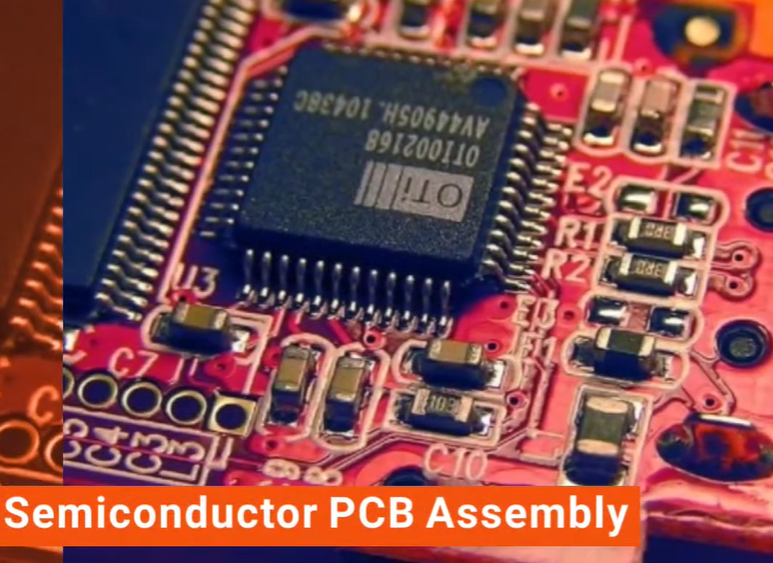
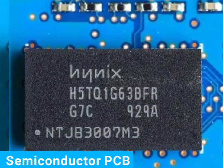
Semiconductor PCB uses semiconductor as the base material, on which other electronic components and semiconductor devices are connected.
Most semiconductor PCBs are relatively small compared to regular PCBs, making them ideal for small appliances such as smart watches.
Semiconductor PCB is also called semiconductor printed circuit board.
Difference between PCB and Semiconductor

PCB (Printed Circuit Board) and semiconductors have their own unique roles and functions in the electronics industry.
First, a semiconductor is a raw material that can control electric current, such as silicon and germanium. Semiconductors are the basic materials for making electronic components, such as transistors, diodes, integrated circuits, etc. These electronic components can be used to control electric current, amplify and process electronic signals.
PCB is a plate made of conductive material on which some circuits and other component structures are formed to realize electrical connections between electronic components. Unlike semiconductors, PCB is not a raw material, but a basic component that connects various electronic components. The design and manufacturing of PCB is crucial to the realization of electronic products. It not only allows various electronic components to be connected, but also fixes the position and connection method of components in circuit design.
Although PCBs and semiconductors have obvious differences in definition and function, they complement each other in electronic products. Semiconductor devices such as transistors are widely used in PCBs. These devices are supported and connected through PCB boards to form a complete circuit.
Overall, PCBs and semiconductors each have their own unique role in the electronics industry. Semiconductors, as basic materials, are mainly used to make various electronic components; PCB, as a basic component, is mainly used to realize electrical connections between electronic components. In practical applications, the two often need to cooperate with each other to realize the functions of electronic products.
Semiconductor PCB materials
Semiconductor PCB materials mainly include FR-4, PP semi-solid sheets, Core core boards, etc. Among them, the Core board is composed of copper foil, solid resin material and glass fiber, and has a certain hardness and thickness. The PP semi-solid sheet is composed of semi-solid resin material and glass fiber, and is mainly used to fill the adhesive material and insulating material of the inner conductive pattern of multi-layer printed boards.
In addition, there are PCBs using silicon carbide materials, which are suitable for high-temperature circuit boards because of their high thermal conductivity. There are also PCBs using FR-4 material, which has good insulation properties, mechanical strength and thermal stability.
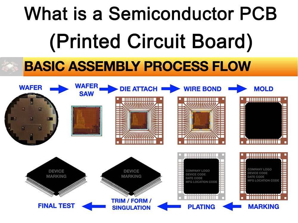
Semiconductor PCB Design
The process of semiconductor PCB (printed circuit board) design includes the following steps:
Determine design requirements
According to specific application requirements, clarify the circuit’s functions, performance indicators, size, cost and other requirements.
Select appropriate substrates and components
According to design requirements, select appropriate substrates and components, such as integrated circuits, transistors, resistors, capacitors, etc.
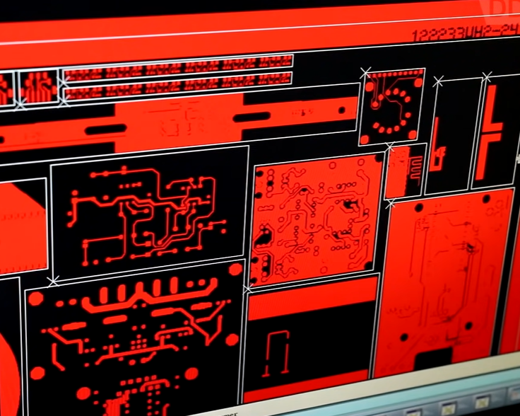
Circuit design
According to the design requirements, use circuit design software to design circuit schematics and PCB layout. In the design, factors such as signal transmission, power distribution, component layout, and wiring direction need to be considered.
Determine PCB specifications and number of layers
Determine PCB specifications and number of layers according to the complexity and size requirements of the circuit. Multilayer PCBs are beneficial to reducing size and cost, but will increase the difficulty of design and manufacturing.
Wiring design
According to the circuit design, use wiring tools to design PCB wiring. In the wiring design, factors such as the direction, width, and spacing of the wiring need to be considered to ensure the normal operation of the circuit.
Verification and optimization
After completing the wiring design, circuit verification and optimization need to be performed to ensure the correctness and reliability of the design. At the same time, the PCB also needs to be optimized to improve its manufacturability and reliability.
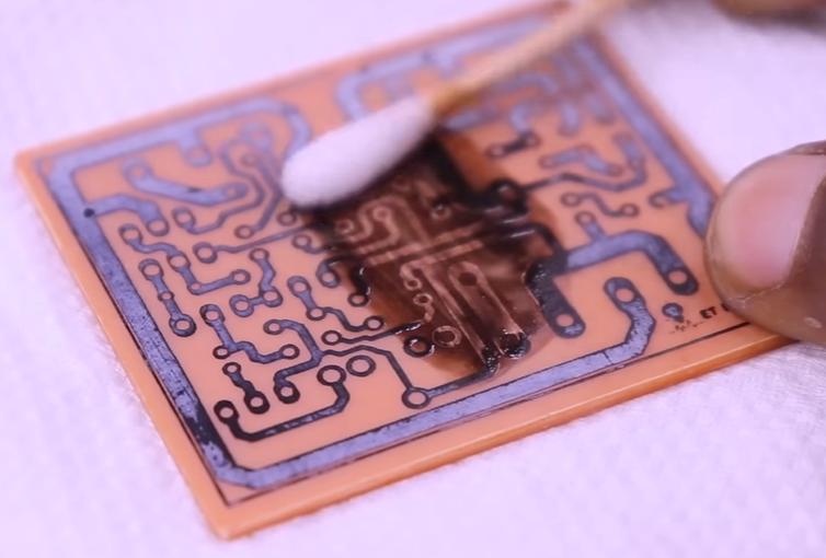
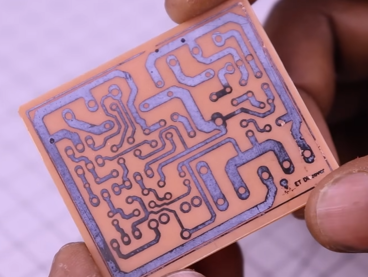
Board making
Submit the designed PCB files to a professional board making factory for production. During the board making process, it is necessary to ensure the quality and accuracy of the board making to ensure the final circuit performance.
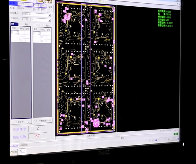
Testing and verification
After completing the board manufacturing, the PCB needs to be tested and verified to ensure that its performance meets the design requirements. If problems are found, corresponding modifications and optimizations need to be made.
Document organization and archiving
Finally, organize the entire design process into documents and archive them for subsequent design reference and use.
During the entire semiconductor PCB design process, it is necessary to comprehensively consider factors such as circuit performance, size, cost, etc., select appropriate substrates and components, and optimize circuit design and wiring design to ensure final circuit performance and reliability. At the same time, attention must be paid to complying with relevant design specifications and standards to ensure the legality and compliance of the design.
Semiconductor PCB Layout
In semiconductor PCB layout, the following factors need to be considered:
Component layout
Follow the layout principle of “large first, then small, difficult first, easy later”, that is, important unit circuits and core components should be laid out first.
At the same time, refer to the schematic block diagram and arrange the main components according to the main signal flow pattern of the single board.
In addition, the arrangement of components should be convenient for debugging and maintenance, that is, large components should not be placed around small components, and there should be enough space around components that need to be debugged.
Circuit board size
Determine the optimal shape and size of the circuit board based on the function and complexity of the circuit board, as well as the actual number of components that need to be carried.
Process requirements
According to the requirements of the production process, determine the layout and wiring method of the PCB. For example, in a multi-layer PCB, the signal routing and connection methods between the layers, as well as the distribution of power and ground, need to be considered.
Thermal design
Thermal design needs to be considered during layout. According to factors such as the heat generation and heat dissipation conditions of the components, the locations of the components should be reasonably arranged and appropriate heat dissipation measures should be taken.
Electromagnetic compatibility
Electromagnetic compatibility needs to be considered during layout, and the location and routing of components should be reasonably arranged to reduce electromagnetic interference and noise.
Reliability
Reliability needs to be considered during layout and appropriate measures should be taken to improve the reliability and stability of the circuit board. For example, redundant design of key components, adding power filters, etc.
In short, semiconductor PCB layout needs to consider multiple factors to ensure that the circuit board has good performance, reliability and stability. At the same time, layout solutions need to be continuously optimized and improved to improve production efficiency and quality.
Semiconductor PCB functional characteristics
Semiconductor PCB (Printed Circuit Board) is a circuit board with semiconductor devices. Its functional characteristics mainly include the following aspects:
High-density integration
Semiconductor PCB uses high-density wiring technology, which can integrate a large number of electronic components and wires into one, and has the characteristics of high density and miniaturization.
High reliability
Semiconductor PCB uses high-quality substrates and advanced process technology, has good electrical performance and stability, and can ensure high-reliability circuit connections and signal transmission.
High efficiency
The high-density integration and short-line connection design of semiconductor PCB can reduce the delay and loss of signal transmission and improve the working efficiency of the circuit.
Good heat dissipation performance
The semiconductor devices on the semiconductor PCB will generate heat, and the base material of the PCB has good thermal conductivity, which can quickly conduct the heat out and ensure the normal operating temperature of the electronic components.
Easy to maintain and upgrade
The electronic components and circuits on the semiconductor PCB are standardized and easy to maintain and upgrade. At the same time, the design and manufacturing process of PCB also make it have good repairability and replaceability.
Diversified application fields
Semiconductor PCB has a wide range of application fields, including communications, computers, consumer electronics, automotive electronics, etc., which can meet the needs of different fields.
In general, semiconductor PCB has the characteristics of high-density integration, high reliability, high efficiency, good heat dissipation performance, easy maintenance and upgrade, and diversified application fields. It is one of the indispensable and important components in modern electronic equipment. .
Development History of Semiconductor PCB
The development history of PCB (Printed Circuit Board) can be traced back to the early 20th century, and the emergence and application of semiconductors occurred decades after that. The following is the development history of semiconductor PCB:
Early exploration stage (1900-1940s)
In the early 20th century, people began to explore circuit connections in electronic devices. At this stage, any electronic device contains many wires, which not only get tangled together and take up a lot of space, but short circuits are not uncommon. German inventor Albert Hansen pioneered the concept of using “wires” for telephone switching systems in 1903 and conceived the idea of metal foil being used to cut line conductors. These early explorations laid the foundation for later PCB inventions.
PCB Enlightenment Stage (1920s-1940s)
In the 1920s, American inventor Charles Ducas printed circuit patterns on insulating substrates, and then used electroplating to create conductors for wiring. It is a symbol of opening up modern PCB technology. In 1936, Paul Eisler published foil technology in the UK. He used a printed circuit board in a radio device, which is considered the world’s first true PCB. In the same year, Japan’s Miyamoto Kinosuke successfully applied for a patent for the spray-on wiring method “Micro Blowing Wiring Method (Patent No. 119384)”. By 1943, Americans used this technology extensively in military radios.
Rapid development stage (1950s-1980s)
With the recovery of the post-war economy and the rapid development of the electronics industry, PCB manufacturing technology and semiconductor technology began to develop rapidly. In 1953, Motorola developed a double-sided panel with electroplated through-holes and later applied it to multi-layer circuit boards.
By 1960, V. Dahlgreen used metal foil film with printed circuits attached to plastic to create a flexible printed circuit board. In 1961, the Hazeltine Corporation in the United States made reference to the electroplating through-hole method and produced multilayer boards.
Since then, with the continuous advancement of technology and the expansion of the market, PCB and semiconductors have gradually become an important part of the electronics industry.
Modern application stage (1990s to present)
As electronic products continue to become miniaturized and intelligent, the design and manufacturing technology of PCB and semiconductors also continue to advance. In 1995 and 1996, Panasonic and Toshiba developed ALIVH and B2IT build-up printed circuit boards respectively.
After entering the 21st century, the application fields of PCB and semiconductors have further expanded, involving communications, computers, consumer electronics, automotive electronics, medical electronics and other fields.
At the same time, the application of emerging technologies such as green manufacturing and smart manufacturing also provides new opportunities for the sustainable development of PCBs and semiconductors.
In general, the development of PCB and semiconductors complements each other. As the support and connection basis of electronic products, PCB provides a reliable installation platform and circuit channel for semiconductor devices; and the continuous expansion of semiconductor performance and application fields also provides PCB with more functions and higher integration. In the future, with the continuous development of technology, PCB and semiconductors will continue to drive the development and innovation of the electronics industry.
What is a semiconductor pcb used for
Semiconductor PCBs are widely used in many fields. Here are some common uses:
- Electronic equipment manufacturing: PCB is an important part of electronic equipment manufacturing. It is used to connect electronic components together to achieve circuit control and communication.
- Automobile industry: In the automobile industry, PCB is widely used in control systems, such as engine control, brake system control, etc.
- Military industry: In the military industry, PCB is used in various military equipment, such as radars, missile control systems, etc.
- Medical equipment: Many medical equipment, such as heart monitors, medical crutches, etc., use PCB technology to achieve more efficient signal control.
- Consumer electronics: PCB boards are widely used in the manufacturing of consumer electronics such as mobile phones, laptops, tablets, etc.
In short, semiconductor PCB has a wide range of uses and plays an important role in promoting the development of modern industry.
Application of semiconductor PCB in medical field
In the medical field, the application of semiconductor PCB is mainly reflected in the manufacturing of medical equipment. Medical equipment requires high-precision and high-reliability circuit boards to support its operation, and semiconductor PCBs precisely meet these requirements.
For example, in medical imaging equipment, such as CT, MRI and X-ray machines, PCBs are used to receive and transmit image signals to ensure the normal operation of the equipment and the accuracy of diagnosis. In addition, in monitoring equipment, such as electrocardiographs, blood pressure monitors, and blood glucose meters, PCBs also play a key role in collecting, processing, and transmitting physiological data.
In medical devices, such as pacemakers, implantable defibrillators, and neurostimulators, PCBs are an integral part. These devices need to be implanted into the human body for a long time, so the PCB is required to have extremely high reliability and stability.
In general, semiconductor PCBs are widely used in the medical field and play an important role in improving the performance and reliability of medical equipment and ensuring patient safety.
Application of semiconductor PCB in automotive field
In the automotive field, the application of semiconductor PCB is equally important. Here are some specific examples:
Engine control unit (ECU)
ECU is the key control center of the automobile engine. It is responsible for receiving various sensor signals and issuing instructions to control the work of the engine. PCB plays a core role in the ECU and is used to implement signal processing and transmission.
Vehicle infotainment systems
These systems include center console displays, audio equipment, navigation systems, etc. They require complex PCB boards to support various functions.
Air conditioning control module
By controlling parameters such as fan speed and temperature, the PCB maintains a comfortable temperature in the car.
Safety systems
Such as the airbag control module, which is responsible for monitoring the situation and inflating when needed to protect passengers in the event of a collision.
Anti-lock braking system (ABS)
ABS prevents wheels from locking by monitoring the speed of the wheels and adjusting the braking force. PCB is also used in this.
Sensor module: includes various sensors, such as temperature sensor, pressure sensor, light sensor, etc., which are used to monitor vehicle status and transmit data to the on-board computer.
Electric seat control module
This module controls the adjustment of the electric seat, including seat height, front and rear, tilt, etc.
Lighting control module
This module controls the lighting system inside and outside the car, including headlights, position lights, interior lighting, etc.
Body control module
This module is responsible for monitoring the status of the body, such as door status, window status, etc., and executing corresponding control actions.
Charging control module
For electric vehicles, this module is responsible for charging management and protection of the battery.
Driving assistance systems
Such as autonomous driving, reversing imaging, automatic parking, etc. These systems require complex electronic control and sensor support, and PCB is the key component to achieve these functions.
The above are some applications of semiconductor PCBs in the automotive field.
What is a Semiconductor PCB vs PCB
PCB (printed circuit board) and semiconductor PCB have their own unique roles in the electronics industry.
PCB is a plate made of conductive material on which some circuits and other components are formed to realize electrical connections between electronic components. It is the support body of electronic components and the carrier of electrical connections between electronic components, providing an indispensable foundation for the realization of electronic products. In addition, it not only allows various electronic components to be connected, but also can fix the position and connection method of components in circuit design.
Semiconductor PCB uses an empty PCB board to undergo processes such as SMT patching, DIP plug-in and testing to form a finished product, referred to as PCBA for short. It installs semiconductor devices on a PCB to form a complete circuit. Compared with PCB, semiconductor PCB goes one step further. It implements more electronic functions by installing various semiconductor devices, such as integrated circuits, transistors, diodes, etc., on the PCB.
Therefore, there are obvious differences in definition and function between PCB and semiconductor PCB. PCB is a basic electronic component, mainly used to support and connect electronic components; while semiconductor PCB further integrates semiconductor devices on the basis of PCB to achieve more complex electronic functions. In practical applications, the two often need to cooperate with each other to achieve the best performance of electronic products.
In general, PCB and semiconductor PCB each have their own unique role in the electronics industry. Although semiconductor PCBs are more complex in function, PCBs also play an indispensable role in electronic products as basic components. In practical applications, it is very important to choose the appropriate circuit board type according to different needs.
Which is more powerful, semiconductor or PCB?
Semiconductors and PCBs each play an important role in the electronics industry and have different advantages and characteristics, so they cannot be compared simply.
Semiconductors are core components of electronic products, capable of controlling electrical current to achieve various electronic functions. Semiconductors are widely used in the electronics industry, including integrated circuits, transistors, diodes, etc. With the development of technology, the performance of semiconductors continues to improve, and the application fields continue to expand.
PCB is the support and connection basis of electronic products. It can connect various electronic components to form a complete circuit. PCB design and manufacturing are critical to the performance and stability of electronic products. In the R&D and production of electronic products, the design and manufacturing of PCBs need to work closely with the design and manufacturing of semiconductors to ensure the correctness and reliability of the circuits.
Therefore, both semiconductors and PCBs are important parts of the electronics industry, each with its own unique advantages and characteristics. In practical applications, the two often need to cooperate with each other to achieve the best performance of electronic products. Today, with the rapid development of technology, the performance and application fields of semiconductors are constantly expanding, and PCB design and manufacturing technology are also constantly improving, both of which are driving the development of the electronics industry.
PCB or semiconductor PCB, which one is more expensive?
In terms of price, semiconductor PCB and PCB each have their own characteristics and factors that affect their cost and price.
Generally speaking, PCB design and manufacturing are relatively simple, so the price is relatively low. Semiconductor PCB further integrates semiconductor devices on the basis of PCB. Its manufacturing cost is relatively high, so the price is also relatively high.
In addition, the prices of PCBs and semiconductor PCBs are also affected by factors such as different types, specifications, quality and workmanship. For example, high-density interconnect (HDI) PCB has the characteristics of high density, high performance and miniaturization, and its manufacturing cost and price are relatively high, while simple FR4 PCB is relatively low. In addition, different production scales and market demands will also affect prices.
Therefore, it is impossible to simply compare whether PCB or semiconductor PCB is more expensive. Different factors and specific situations need to be considered comprehensively. When choosing a circuit board, you need to weigh the actual needs and budget to choose the most suitable circuit board type.
Semiconductor PCB FAQs
PCB (Printed Circuit Board), that is, printed circuit board, is the support for electronic components and the connection basis for electronic circuits.
Semiconductor PCB is based on ordinary PCB and integrates semiconductor devices, such as integrated circuits, transistors, diodes, etc., to form a circuit board with specific functions.
The characteristics of semiconductor PCB include high-density integration, high reliability, high efficiency, good heat dissipation performance, easy maintenance and upgrade, and diverse application fields.
Semiconductor PCB is widely used in communications, computers, consumer electronics, automotive electronics and other fields, and is an indispensable and important component in modern electronic equipment.
PCB short circuit problems may be caused by improper soldering pad design, improper part orientation design, automatic plug-in bent feet, etc. Solutions include modifying the pad design, part orientation, or modifying the automatic plug-in bending feet.
To avoid PCB corrosion traps, the angle between leads should be minimized to avoid sharp angles. At the same time, the use of modern manufacturing processes such as photosensitive etching solutions can also greatly reduce the formation of corrosion traps.
Tombstone device problems are often caused by asymmetric wiring patterns that spread heat unevenly across the device pads. Solutions include optimizing routing patterns so that heat spreads evenly across the device pads.
Layout is an important part of PCB design. Reasonable layout can improve circuit performance and reduce costs. Solutions include laying out the core components of each functional circuit as the center. The components should be arranged evenly, neatly and compactly on the PCB, minimizing and shortening the leads and connections between components, and arranging each component according to the flow of the circuit. The location of functional circuit units, etc.
To ensure the reliability of PCB, we need to start from many aspects, including selecting appropriate substrates and components, optimizing design, improving process accuracy, strengthening quality management, etc. In addition, regular maintenance and inspection are also important measures to ensure the reliability of PCB.