
A triode is an electronic component made on a semiconductor substrate. It consists of two PN junctions that are very close to each other.
These three parts divide the entire semiconductor into three parts: base area, emitter area and collector area.
Depending on the arrangement of the semiconductor materials, there are two types of transistors: PNP and NPN.
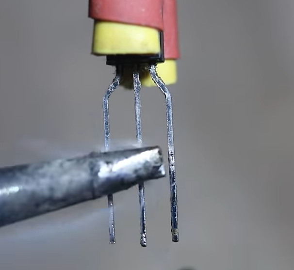
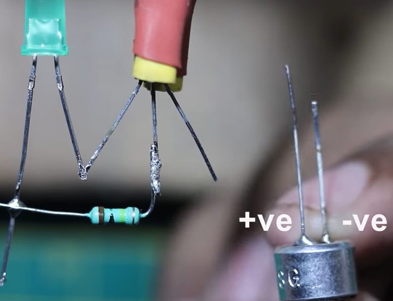
The pin design of the triode means that the triode has three pins, which are the base (Base, referred to as B), the collector (Collector, referred to as C) and the emitter (Emitter, referred to as E).
Transistor pin design core
These three pins correspond to the three areas inside the triode, and each pin has its specific function and role.
Base (B):
The base is the control electrode of the triode. It controls the amplification of the triode by controlling the input of current. Small changes in the base current will cause large changes in the collector current, thereby achieving current amplification.
Collector (C):
The collector is the main output terminal of the triode. It is responsible for collecting and outputting the amplified current. When the triode is working, a certain voltage needs to be applied between the collector and the emitter to maintain the normal operation of the triode.
Emitter (E):
The emitter is another important output terminal of the triode. It forms a PN junction together with the base and collector to achieve current amplification. The current change of the emitter is controlled by the base current. When the base current increases, the emitter current will also increase accordingly.
In the actual application of triodes, the pin design allows the triode to be easily connected and combined with other electronic components to achieve various complex circuit functions.
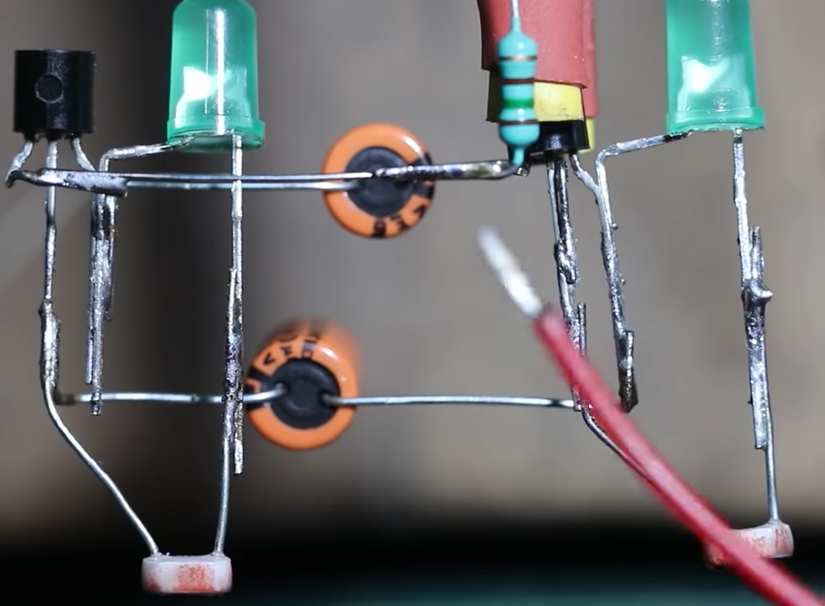
For example, in the microcontroller application circuit, the triode mainly plays the role of a switch, controlling the on-off of the entire circuit by controlling the on-off of the base current. In addition, triodes can also be used for circuit functions such as signal amplification and modulation.
Why do we need to design the pins of the triode?
The pins of the transistor are designed for efficient connection and utilization. First of all, through reasonable pin design, reliable connection between the triode and other electronic components can be achieved to ensure the stability and reliability of the circuit. Secondly, the pin design can optimize the input and output of current and signals, thereby optimizing the working efficiency and performance of the triode. In addition, reasonable pin design can also facilitate the detection, repair and replacement of triodes, improving the maintainability and reliability of electronic equipment. In short, the pins of the triode are designed to meet various needs in practical applications and to achieve efficient, stable and reliable operation of electronic equipment.
How are the pins of the triode designed?
The transistor is a common electronic component with three electrodes, namely base b, collector c and emitter e.
In terms of pin design of transistors, certain standards are generally followed to ensure compatibility with other components and circuits.
Here are some key points about transistor pin design:
- Pin arrangement: The pin arrangement sequence of triodes is usually determined according to international standards. Normally, the three pins of a triode are arranged in a certain order, usually in the order of base, collector and emitter. In circuit diagrams, they are also labeled and annotated in this order.
- Pin function: The function of each pin is specific. The base is the control electrode, the collector is the input electrode, and the emitter is the output electrode. In the circuit, by controlling the size of the base current, the current flow between the collector and the emitter can be controlled, thereby achieving functions such as signal amplification and switching control.
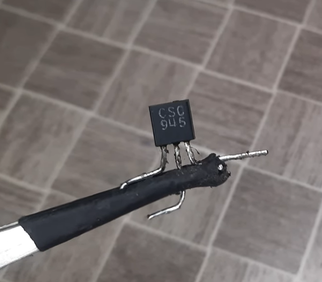
- Package type: There are many package types of transistors, and each package type has different pin arrangements and sizes. For example, TO-92 packaging, TO-220 packaging, SOT-23 packaging, etc. When designing these package types, factors such as pin arrangement, pin spacing, and pin length need to be considered to ensure that the components can be successfully installed on the circuit board.
- Pin spacing: Pin spacing refers to the distance between two adjacent pins. The size of this distance has a certain impact on the installation of components and the layout of the circuit board. Generally speaking, the larger the pin spacing, the easier it is to install and solder components, and it will also help improve the anti-interference performance of the circuit board.
- Lead length: Lead length is the length from the bottom of the component to the top of the lead. When selecting the pin length, two factors need to be considered: one is the convenience during soldering, and the other is the space for the circuit board layout. If the pin length is too long, it may cause problems such as instability during soldering or short circuits with other components; if the pin length is too short, it may affect the layout and routing of the circuit board.
When designing the transistor pins, you also need to pay attention to the following points:
- Consider package type and size: Different package types have different sizes and pin arrangements. You need to choose the appropriate package type and size according to actual needs.
- Consider circuit board layout and wiring: When selecting pin length and spacing, you need to consider the needs of circuit board layout and wiring to ensure the stability of component installation and the reliability of circuit performance.
- Follow standards: When designing pins, international standards and industry specifications should be followed to ensure that the designed transistor is compatible with other components and circuits.
- Conduct simulation and testing: During the design process, simulation and testing can be performed to verify the feasibility and reliability of the design. This helps reduce errors and defects in the design and improves the success rate of the design.
In short, transistor pin design is a process that requires consideration of multiple factors. In the design, multiple aspects such as package type, functional requirements, circuit board layout, and standard specifications should be comprehensively considered.
Through reasonable design, the stability and reliability of the triode in the circuit can be ensured, thereby improving the performance and quality of the entire circuit.
International standards
There is no unified international standard for transistor pin design, because different manufacturers and different application scenarios may use different pin arrangement sequences. However, there are some common pin ordering and labeling methods to facilitate user understanding and use.
A common pin arrangement is the TO-92 packaged triode, whose pin arrangement is base, collector, and emitter. On the pins of the TO-92 package, the numbers 1, 2, and 3 are usually marked, corresponding to the base, collector, and emitter respectively. In addition, the letters B, C, and E are also marked on the pins of some triodes, which represent the base, collector, and emitter respectively.
Another common pin arrangement is the SOT-23 packaged transistor, whose pin arrangement is emitter, base, collector. On the pins of the SOT-23 package, the numbers 1, 2, and 3 are usually marked, corresponding to the emitter, base, and collector respectively. In addition, the letters E, B, and C are also marked on the pins of some triodes, which represent the emitter, base, and collector respectively.
In addition to the common pin arrangement order and labeling methods, there are also some special transistors that may use non-standard pin arrangement order and labeling methods. Therefore, when selecting and using a triode, users need to carefully check the triode’s specification sheet or circuit diagram to ensure correct connection and use.
It should be noted that the pin arrangement of transistors from different manufacturers may be different. Therefore, in actual use, it is necessary to carefully check the pin arrangement and labeling of the transistors to avoid connection errors that may cause abnormal circuit operation. At the same time, for some special application scenarios and specially packaged transistors, users need to select and use them according to specific requirements.
Transistor pin design FAQs
The main function of the triode is current amplification.
The manufacturing process of the emitter and collector of the triode is not symmetrical, and its structure is not symmetrical. If replaced, the amplification capacity will be much smaller than before replacement, and the pressure resistance will also be much smaller.
When working in the amplification zone, the collector is in a reverse biased state. At this time, if the base lead is disconnected and U_{CE} is large during operation, the collector junction may be broken down due to excessive reverse voltage.
Generally divided into amplification area, saturation area and cut-off area.
There are three basic configurations of amplifier circuits, namely common emitter, common base and common collector.
In the common emitter amplifier circuit, there are three types of bias circuits: upper base bias, voltage divider type and set-base feedback type.
It should usually be in the center of the amplification area of the triode’s input-output characteristic curve.
Correctly determining the static operating point enables the amplifier to have minimum cutoff distortion and saturation distortion, while also obtaining the maximum dynamic range and improving the efficiency of the triode.
The emitter of a transistor is usually made of N-type silicon material, that is, the silicon material is doped with a small amount of pentavalent elements, such as phosphorus (P) or arsenic (As). These materials have an excess of free electrons and therefore have high electrical conductivity.
However, in actual applications, other materials may be used to make the emitter depending on the specific purpose and performance requirements of the triode. For example, in some high-frequency applications, materials such as gallium arsenide (GaAs) or indium phosphide (InP) may be used to make the emitter. These materials have higher carrier mobility and shorter carrier lifetime, providing higher emission efficiency and frequency response.
The base material of the triode is usually silicon (Si). Silicon is a common semiconductor material with good electrical conductivity and thermal stability. Silicon material has a high energy band width, which allows it to operate at room temperature and is suitable for most electronic devices. Silicon materials also have high electron mobility and low electron affinity, allowing triodes to achieve high-frequency amplification and switching operations.
The collector of a transistor is usually made of N-type silicon material, that is, the silicon material is doped with a small amount of pentavalent elements, such as phosphorus (P) or arsenic (As). N-type silicon materials have excess free electrons and therefore have higher conductivity.