
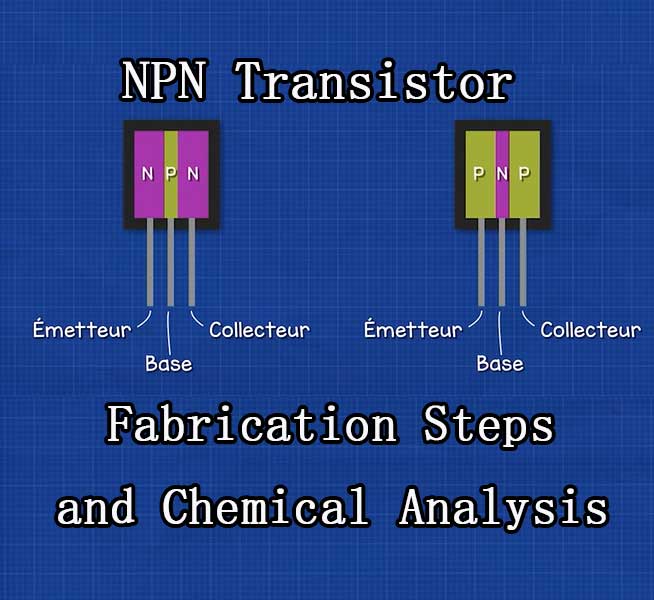
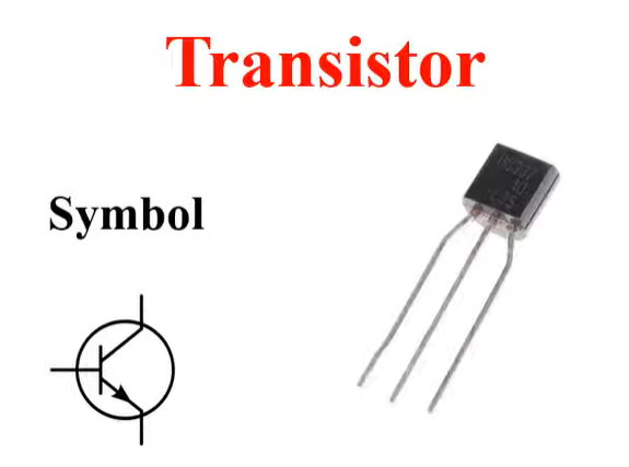
NPN transistors are three-terminal semiconductor devices consisting of a base, an emitter, and a collector. It is one of the most important components in electronic circuits and is used for amplification, switching and logic operations.
The manufacturing process of NPN transistors is divided into the following steps:
Substrate selection
- Select the appropriate substrate material, such as silicon wafer, germanium wafer, etc., according to the specifications and application requirements of the transistor.
- Consider the mechanical properties, thermal stability, chemical stability and compatibility with subsequent processes of the substrate.
surface treatment
- Clean the substrate to remove surface impurities and contaminants.
- Carry out oxidation or nitriding treatment to form a protective layer and improve surface properties.
crystal growth
- Use physical vapor deposition, chemical vapor deposition and other methods to grow single crystal materials on the selected substrate.
- Control parameters such as temperature, pressure, air flow, etc. to ensure the quality and stability of crystal growth.
transistor doping
- The required impurities are introduced into the crystal by methods such as ion implantation, diffusion or chemical vapor deposition.
- The purpose of doping is to form a conductive channel and control the conductive performance of the transistor.
Transistors make PN junctions
- Perform photolithography, etching and other processes on the crystal surface to form a PN junction structure.
- The PN junction is formed through heat treatment or chemical treatment.
Transistor electrode manufacturing
- Make metal electrodes on the crystal surface to realize current input and output.
- Select appropriate metal materials and process conditions to ensure good contact between the electrode and the crystal material.
Transistor packaging testing
- Encapsulate the transistor in a suitable casing to protect it from the external environment.
- Conduct electrical performance testing to ensure the normal function and stable performance of the transistor.
Chemical analysis of NPN transistors
Ingredient analysis
- Determine the types and contents of various elements in the crystal through mass spectrometer (MS) or X-ray fluorescence spectrometer (XRF).
- Determine the distribution and concentration of impurity elements and evaluate their impact on transistor performance.
Chemical bonding state analysis

- Use infrared spectroscopy (IR) technology to analyze the chemical bonding state in the crystal.
- Understand the role of different chemical bonds in crystals and their impact on transistor performance.
Surface chemical analysis
- Use techniques such as atomic force microscopy (AFM) and X-ray photoelectron spectroscopy (XPS) to analyze the chemical properties and element distribution on the crystal surface.
- Understand the presence of surface contaminants and their impact on transistor performance.
Chemical stability analysis
- Evaluate the stability of crystals under different temperatures and atmospheres through thermogravimetric analysis (TGA), differential thermal analysis (DSC) and other methods.
- Analyze the performance changes of crystals in harsh environments to provide basis for their application.

Comprehensive analysis methods combined with computer simulation technology
Build more accurate models to predict and optimize transistor performance.
Through the above introduction of manufacturing steps and chemical analysis, we can better understand the manufacturing process and performance characteristics of NPN transistors, and provide guidance for actual production and application.
Chemical analysis of NPN transistors can be used to determine their structure and composition. Commonly used analysis methods include:
Energy spectroscopy
Energy spectroscopy can be used to determine the content of elements in a transistor.
Spectroscopy
Spectroscopy can be used to determine the type and concentration of impurities in a transistor.
Electrochemical analysis
Electrochemical analysis can be used to determine the doping type and concentration of a transistor.
These analytical methods help manufacturers ensure that transistors meet required characteristics.
What instruments and equipment are needed for chemical analysis of NPN transistors?
When performing chemical analysis of NPN transistors, you may need to use the following instruments and equipment:
electron microscope
Used to observe the microstructure of the crystal surface and interior.
X-ray diffractometer
It is used to determine the crystal structure and analyze the atomic spacing and relative content of various elements in the crystal.
infrared spectrometer
Used to determine chemical bonds and molecular structure in crystals.
atomic force microscope
Used to analyze the morphology and chemical properties of crystal surfaces.
mass spectrometer
Used to determine the relative content of elements in crystals.
Electronic energy spectrometer
Used to analyze the chemical state and electronic structure of crystal surface elements.
These instruments can help us deeply understand the chemical and physical properties of NPN transistors, thereby optimizing their performance and improving their reliability.