
Bipolar transistors have many parameter symbols and their meanings. For example, B, C, and E represent the base, collector, and emitter respectively. Ib, Ic, and Ie represent the currents of the base, collector, and emitter, respectively, while Vcb, Vbe , Vce represents the voltage between the collector and the base, the emitter and the base, and the collector and the emitter.
Together, these parameter symbols define the operating characteristics of a bipolar transistor and are critical to understanding its performance and how it is used.
Bipolar transistor is a common electronic device. Its parameter symbols and their meanings are as follows:
- Ic: collector current, refers to the DC current passing through the collector of the transistor under given conditions. The average value of collector DC or AC current.
- Icbo: The reverse saturation current between the base and collector when the emitter is open circuit. The base is grounded, the emitter is open to ground, and the reverse cut-off current between the collector and the base under the specified VCB reverse voltage condition
- Iceo: The reverse blocking current between the emitter and collector when the base is open circuit at a given temperature. The emitter is connected to ground and the base is open to ground. Under the specified reverse voltage VCE condition, the reverse cut-off current between the collector and emitter is reached.
- Iebo: Reverse cutoff current between base and emitter when collector is open circuit at a given temperature. The base is grounded, the collector is open to ground, and under the specified reverse voltage VEB condition, the reverse cut-off current between the emitter and the base is reached.
- IB: The average value of base DC current or AC current
- IE: the average value of the emitter DC current or AC current
- Icer: The series resistor R between the base and the emitter. When the voltage VCE between the collector and the emitter is a specified value, the reverse cut-off current between the collector and the emitter is
- Ices: The emitter is grounded, the base is short-circuited to ground, and under the specified reverse voltage VCE condition, the reverse cut-off current between the collector and the emitter
- Icex: The emitter is grounded, a specified bias voltage is applied between the base and the emitter, and under the specified reverse bias voltage VCE, the reverse cut-off current between the collector and the emitter
- ICM: The maximum allowable current of the collector or the maximum average value of the AC current.
- IBM: The maximum value of DC current that can continuously pass through the base within the range that the collector is allowed to dissipate power, or the maximum average value of AC current
- ICMP: collector maximum allowable pulse current
- ISB: secondary breakdown current
- IAGC: forward automatic current control
- Pc: collector dissipation power, which refers to the maximum power that the transistor can withstand during normal operation.
- PCM: The maximum allowable power dissipation of the collector refers to the maximum power dissipation that the transistor can withstand under given conditions.
- Pi: input power
- Po: output power
- Posc: oscillation power
- Pn: noise power
- Ptot: total power dissipated
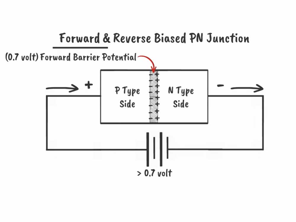
- VCB: Reverse breakdown voltage between collector and base.
- VBE (Vb): forward voltage between base and emitter.
- VCEO: Reverse breakdown voltage between collector and emitter.
- VCES: Saturation voltage between collector and emitter.
- β: Common base amplification factor, which refers to the ratio of the change of the output signal to the change of the input signal in the common base circuit.
- α: Common emitter amplification factor, which refers to the ratio of the change amount of the output signal to the change amount of the input signal in the common emitter circuit.
- fT: Characteristic frequency of the transistor, which refers to the highest operating frequency of the transistor.
- fmax: The limit frequency of the transistor, which refers to the highest frequency at which the transistor can operate normally. The operating frequency when the triode power gain is equal to 1.
- fmin: The lowest operating frequency of the transistor, which refers to the lowest frequency at which the transistor can operate normally.
- fα: Common emitter cutoff frequency, which refers to the frequency point at which the amplification factor begins to decrease when the frequency of the input signal increases in the common emitter circuit.
- fβ: The turning frequency of the frequency response of the common emitter signal source, which refers to the frequency point at which the amplification factor begins to decrease when the frequency of the input signal increases in the common emitter circuit.
- fH: Common base cutoff frequency, which refers to the frequency point at which the amplification factor begins to decrease when the frequency of the input signal increases in the common base circuit.
- fL: The turning frequency of the frequency response of the common base signal source, which refers to the frequency point at which the amplification factor begins to decrease when the frequency of the input signal increases in the common base circuit.
- Vf: forward voltage drop, refers to the forward conduction voltage of the transistor.
- Vr: Reverse voltage drop, refers to the reverse conduction voltage of the transistor.
- VCB: collector-base (DC) voltage
- VCE: collector-emitter (DC) voltage
- VBE: Base-emitter (DC) voltage
- VCBO: The base is grounded, the emitter is open to ground, and the maximum withstand voltage between the collector and the base under specified conditions
- VEBO: The base is grounded, the collector is open to ground, and the maximum withstand voltage between the emitter and the base under specified conditions
- VCEO: The emitter is grounded, the base is open to ground, and the maximum withstand voltage between the collector and emitter under specified conditions
- VCER: The emitter is grounded, a resistor R is connected in series between the base and the emitter, and the maximum withstand voltage between the collector and the emitter under specified conditions
- VCES: The emitter is grounded, the base is short-circuited to ground, and the maximum withstand voltage between the collector and emitter under specified conditions
- VCEX: The emitter is grounded, a specified bias voltage is applied between the base and the emitter, and the maximum withstand voltage between the collector and the emitter under specified conditions
- Vp: punch-through voltage.
- VSB: Secondary breakdown voltage
- VBB: Base (DC) power supply voltage (external circuit parameters)
- Vcc: Collector (DC) power supply voltage (external circuit parameters)
- VEE: Emitter (DC) power supply voltage (external circuit parameters)
- VCE(sat): The emitter is grounded, and the saturation voltage drop between the collector and the emitter under Ic and IB conditions is specified.
- VBE(sat): The emitter is grounded, and under specified Ic and IB conditions, the base-emitter saturation voltage drop (forward voltage drop)
- VAGC: forward automatic gain control voltage
- Vn(p-p): Peak equivalent noise voltage at the input end
- V n: noise voltage
- D: duty cycle
- Bvceo: Reverse breakdown voltage, which refers to the maximum reverse voltage between the base and collector of a transistor during normal operation.
- BVcbo: open emitter, breakdown voltage between collector and base
- Bvbeo: Forward breakdown voltage refers to the maximum forward voltage between the base and emitter of a transistor during normal operation.
- Bvces: saturation voltage drop, refers to the voltage drop between the base and emitter of the transistor when it is in saturation state. Base and emitter short circuit CE junction breakdown voltage.
- BVebo: Open collector EB junction breakdown voltage.
- BV cer: The base and emitter are connected in series with a resistor, CE junction breakdown voltage.
- αF: forward current amplification factor, refers to the forward current amplification coefficient of the transistor.
- αR: Reverse current amplification factor, which refers to the reverse current amplification coefficient of the transistor.
- fmaxF: forward maximum operating frequency, refers to the upper limit of the forward operating frequency of the transistor.
- fmaxR: reverse maximum operating frequency, which refers to the upper limit of the reverse operating frequency of the transistor.
- fminF: forward minimum operating frequency, refers to the lower limit of the forward operating frequency of the transistor.
- fminR: Reverse minimum operating frequency, which refers to the lower limit of the reverse operating voltage of the transistor.
- Cc: collector capacitance
- Ccb: Capacitance between collector and base
- Cce: emitter ground output capacitance
- Ci: input capacitance
- Cib: common base input capacitance
- Cie: common emitter input capacitance
- Cies: common-emitter short-circuit input capacitance
- Cieo: Common emitter open input capacitance
- Cn: Neutralizing capacitor (external circuit parameters)
- Co: zero bias capacitor
- Cob: common base output capacitor. In the base circuit, the output capacitance between the collector and the base
- Coe: common emitter output capacitance
- Coeo: Common emitter open output capacitor
- Cre: common emitter feedback capacitor
- Cic: collector junction barrier capacitance
- CL: Load capacitance (external circuit parameters)
- Cp: parallel capacitance (external circuit parameters)
- Cj: Junction (interelectrode) capacitance, indicating the total capacitance of the germanium detection diode when a specified bias voltage is applied to both ends of the diode.
- Cjv: bias junction capacitance
- Cjo: zero bias junction capacitance
- Cjo/Cjn: junction capacitance change
- Cs: case capacitance or package capacitance
- Ct: total capacitance
- CTV: voltage temperature coefficient. The ratio of the relative change of the stable voltage to the absolute change of the ambient temperature under the test current
- CTC: Capacitance temperature coefficient
- Cvn: nominal capacitance
- hFE: common emitter quiescent current amplification factor
- hIE: common emitter static input impedance
- hOE: common emitter static output conductance
- h RE: Common emitter static voltage feedback coefficient
- hie: total emission of very small signal short-circuit input impedance
- hre: total emission of very small signal open circuit voltage feedback coefficient
- hfe: total emission of very small signal short-circuit voltage amplification factor
- hoe: total emission of very small signal open circuit output admittance
- ESB: Second breakdown energy
- rbb: base area extended resistance (base area intrinsic resistance)
- rbbCc: base-collector time constant, which is the product of base extension resistance and collector junction capacitance
- rie: input resistance when the emitter is grounded and the AC output is short-circuited
- roe: The output resistance when the emitter is grounded and the AC input is short-circuited when measured under specified VCE, Ic or IE, and frequency conditions.
- RE: External emitter resistor (external circuit parameters)
- RB: External base resistor (external circuit parameters)
- Rc: external collector resistor (external circuit parameters)
- RBE: External base-emitter resistance (external circuit parameters)
- RL: Load resistance (external circuit parameters)
- RG: signal source internal resistance
- Rth: thermal resistance
- Ta: ambient temperature
- Tc: shell temperature
- Ts: junction temperature
- Tjm: maximum allowable junction temperature
- Tstg: storage temperature
- td: delay time
- tr: rise time
- ts: storage time
- tf: fall time
- ton: opening time
- toff: off time
- IF: Forward DC current (forward test current). The current passing through the inter-electrode of the germanium detection diode under the specified forward voltage VF; the maximum operating current (average value) allowed to pass continuously in the sinusoidal half-wave of the silicon rectifier and silicon stack under the specified conditions of use, and the silicon switch The maximum forward DC current allowed to pass through the diode under rated power; the current given when measuring the forward electrical parameters of the Zener diode.
- IF (AV): forward average current
- IFM (IM): Forward peak current (forward maximum current). The maximum forward pulse current allowed through the diode at rated power. LED limits.
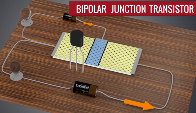
The application scenarios of bipolar transistors mainly include the following aspects:
In the fields of radio, television, communications, radar, computers, automatic control devices, electronic instruments, household appliances, etc., used for amplification, oscillation, switching and other functions.
Traditional industries such as industry, communications, computers, consumer electronics, automotive electronics, aerospace, national defense and military industries, as well as emerging industries such as rail transit, new energy, smart grids, and new energy vehicles.
Constitute amplifier circuits, or drive speakers, motors and other equipment, and are widely used in aerospace engineering, medical equipment, robots and other application products.
As a key component of amplifiers in audio amplification, radio frequency amplification, video amplification and other fields.
Disadvantages of bipolar transistors include temperature sensitivity and bias, which can cause circuit instability. In addition, bipolar transistors may introduce noise that affects circuit performance. In high-speed switching circuits, the response speed of bipolar transistors is relatively slow and is not as stable as field effect transistors. In addition, bipolar transistors consume large amounts of power, require large drive currents, and are relatively large in size.
Despite these shortcomings, bipolar transistors are still used in many fields because of their advantages such as fast response speed, high amplification, and low noise. Choosing the right transistor based on specific needs can improve the performance and stability of your circuit.
The collector currents Ic, Ice, and Ie have the following meanings:
Ic is the limit value, which refers to the collector current, and C represents the collector. The specific meaning of Ic is the maximum DC current of the collector.
Iceo, ICES, and ICER are called transistor collector reverse current. Their names and meanings are as follows: When the emitter is open and a reverse voltage is applied between the collector and the base, the reverse current of the collector is usually called the reverse current. towards saturation current.
Ie represents the current at the emission extreme.
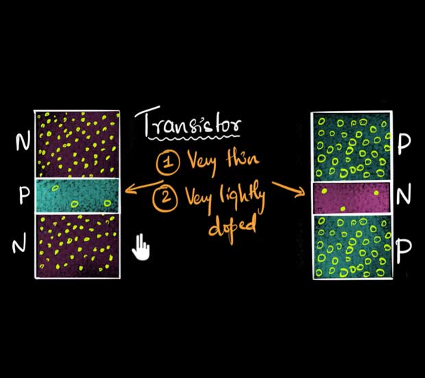
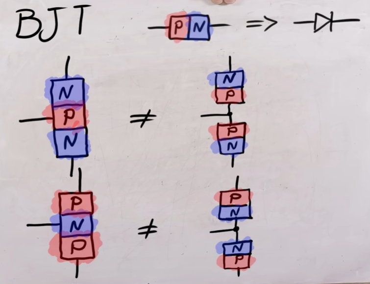
In addition, the transistor has three ports, E emitter, B base and C collector, and I represents the current, IE represents the current at the emitter terminal, IB represents the current at the base terminal, and IC represents the current at the collector terminal.
Bipolar transistors have a wide range of applications, mainly including the following aspects:
Communication field: Bipolar transistors are used for signal amplification, oscillation, switching, etc., and are widely used in radio, television, communications, radar and other fields.
Industrial control field: As a key electronic device, bipolar transistors are used to realize amplification, switching, isolation and other functions of control circuits, and are widely used in industrial automation control systems.
Consumer electronics: Bipolar transistors are used in audio amplification, video amplification, switching circuits, etc., and are key components in many electronic products.
Automotive electronics: Bipolar transistors are used in automotive sensors, ignitions, lighting control and other circuits to function as signal amplification and switching.
Aerospace field: Bipolar transistors have the characteristics of high reliability and long life, and are suitable for various electronic equipment in aerospace engineering.
Medical device field: Bipolar transistors are used in sensors, amplifiers and other circuits in medical devices to perform signal processing and amplification.
Robot field: Bipolar transistors are used in robot control systems and sensor circuits to achieve signal amplification and processing.
Bipolar transistors have a wide range of applications, covering communications, industrial control, consumer electronics, automotive electronics, aerospace, medical equipment and robotics.