2024 China Integrated Circuit Design Innovation Conference

2024 China Integrated Circuit Design Innovation Conference

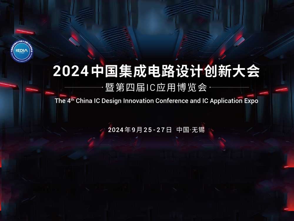
The 2024 China Integrated Circuit Design Innovation Conference will be held at the Wuxi International Convention Center from September 25th to 27th.

The conference focuses on the latest technology, market trends and industry dynamics of integrated circuit design, aiming to promote collaborative innovation and cross-border integration of the industry chain and help the vigorous development of my country’s integrated circuit industry.

Major research institutions believe that after the global semiconductor market reaches a cyclical low in 2023, there will be an overall recovery trend this year.

Gartner predicts that global semiconductor industry revenue will reach US$624 billion in 2024, a year-on-year increase of 16.8%. The storage industry, known as the “barometer” of the semiconductor industry, was the first to experience price increases in the fourth quarter of last year, which has continued into this year and is expected to rebound by 66.3%.

The driving force behind this is the new wave of AI detonated by generative artificial intelligence (AIGC) led by ChatGPT. High-tech companies in data centers, servers, cloud computing, large computing power chips, large models and other fields quickly followed up, forming a new global AI arms race, which directly drove the development of high-bandwidth memory (HBM), GPU and other AI computing power-related technologies. Chip growth.

PBOC Moves, Nvidia Chips | The China Open 01/09/2024

As consumer electronics such as PCs, mobile phones, and tablets continue to recover, the first year of AI PC begins, and the “new four modernizations” of automobiles enter the deep water area, what new changes will occur in the chip industry this year? How to seize the opportunity for recovery? How about upstream and downstream Form a better coordination mechanism?

The 2024 China Integrated Circuit Design Innovation Conference and the 4th IC Application Expo (ICDIA 2024) will be held at the Wuxi International Convention Center from September 25-27. As the top event in China’s IC design industry and electronic technology industry, ICDIA is committed to promoting the application of chips, IC components and systems, and demonstrating China’s core innovation achievements and technological progress.

ICDIA 2024 will focus on the outstanding Chinese chip and innovative applications and achievements, bring eye-catching cutting-edge innovation results to the audience, and display the chip picture of future technology.

With the theme of “Application Innovation, Creating a New Ecosystem”, this conference focuses on the two main lines of “chip industry ecology” and “application-enabled industry upgrading”, with six theme forums, multiple innovation releases and application docking, IC application Exhibition, market-oriented and product-centered to build a supply and demand communication platform for chip applications.

It is worth noting that four large-scale exhibitions on integrated circuit design, packaging and testing, equipment and components, and automotive electronics are gathered at the same time, with a total exhibition area of nearly 50,000 square meters and more than 100,000 professional visitors. It is the largest exhibition for global IC companies and electronic R&D It is the best platform for enterprises to display innovative technologies, explore business opportunities and promote trade cooperation.

Paying attention to innovative applications, promoting application implementation, building a supply and demand platform, and assisting the construction of the chip industry ecosystem are the original intention of ICDIA’s establishment and the characteristics of ICDIA.

Six major theme forums

Create a feast of cutting-edge technology

This conference features six major theme forums, including “Large Models and AI Large Computing Power Chips”, “Low Power Consumption and Embedded Design“, “RSIC-V and IP Applications”, “Chip Cloud and Data Security”, “Communications and Radio Frequency Technology”, “Innovation Release and Application Docking”.

“Low Power Consumption and Embedded Design” Forum

With the continuous deepening of urban informatization and industry intelligence, embedded technology has become one of the fastest growing and most widely used computer technologies in the information industry, and is widely used in consumer electronics, medical electronics, industrial control, and intelligent hardware. In other fields, data from the Ministry of Industry and Information Technology shows that my country’s embedded system software market size will reach 937.6 billion yuan in 2022, a year-on-year increase of 11.04%; it is expected that the embedded system software market size will exceed 1 trillion yuan in 2023.

As digital transformation penetrates into all walks of life and the development of artificial intelligence applications is promoted, low power consumption and high performance will become the core direction of the future development of embedded technology.

This “High Performance Low Power Consumption and Embedded Design” forum will focus on the development and innovative application results of embedded technology in the fields of artificial intelligence, smart terminals, Internet of Things, edge computing, industrial control, etc., and promote the ecological construction of software and hardware systems. Strengthen upstream and downstream communication and collaboration to jointly discuss the future development of embedded systems.

WEP 2024 | CHINA’S ECONOMIC SEQUEL: ROLE OF TECHNOLOGICAL INNOVATIONS IN SHAPING THE FUTURE

“Large Models and AI Big Computing Power Chips” Forum

The explosion of ChatGPT triggered a wave of generative artificial intelligence. Almost at the same time, major Internet high-tech companies were competing to deploy large-scale artificial intelligence model applications and promote the deeper development of artificial intelligence in various fields. In the future, artificial intelligence may change people’s lives. daily life.

With the advent of the era of large artificial intelligence models, the massive demand for computing power has led to arms races one after another in the fields of data centers, servers, and large computing power chips. Data shows that the global AI accelerated computing market will reach US$45 billion in 2023, and is expected to reach US$400 billion by 2027.

This “Large Models and AI Large Computing Power Chips” forum will focus on the development of various large models and the latest application results, AI large computing power chips, including but not limited to GPU, ASIC, CPU, FPGA, GPGPU, etc., aiming to explore The integrated development of large model applications and computing power chips, explores the requirements of different artificial intelligence applications for computing power chips, and the technological development of computing power chips in the post-Moore era including storage and calculation integration and other types of computing structures.

“Cloud on Chip and Data Security” Forum

In the past, most chip design companies focused on local computing power. However, driven by new generation information technologies such as artificial intelligence, 5G, supercomputing, and autonomous driving, chip design is becoming more and more complex, and manufacturing processes are becoming more and more advanced. , the cost has also increased, bringing considerable pressure and challenges to chip design and development.

The use of cloud computing is currently a way to solve the computing power gap faced by chip design and help small and medium-sized enterprises balance costs. Therefore, “chip on the cloud” is becoming a major trend in the chip design industry.

How to get to the cloud? What are the options? How to ensure costs? How to support the “elastic computing power” of chip design? How to ensure security in the semiconductor industry that is extremely sensitive to data?

This “Chip Cloud and Data Security” forum will discuss the above issues, focusing on the situation, difficulties and data security issues of the chip industry’s cloud migration, aiming to establish a communication bridge between the chip industry and cloud service providers, and help build a domestic cloud service ecosystem. Help chip companies find good solutions and make good use of cloud computing to conduct business.

“RISC-V and IP Application” Forum

Since the development of the open source reduced instruction set architecture RISC-V, more and more companies, schools, and scientific research institutes have joined in. RISC-V is more flexible than traditional instruction set architecture, compatible with a wide range of applications, and is mostly used in the field of intelligent Internet of Things. Today, many companies around the world are expanding the RISC-V ecosystem and core applications, covering image sensors, security management, artificial intelligence computing, etc.

Data shows that RISC-V revenue will reach US$800 million in 2023, nearly double the previous two years, and is expected to reach nearly US$1 billion in 2024. As more and more companies embrace the RISC-V ecosystem, they may be able to compete with ARM and x86 in the future.

The open source and open nature of RISC-V will help China break through Western restrictions and achieve independent control. But it is undeniable that RISC-V is still relatively new. Compared with the complete and mature ecology of ARM and x86, it also faces problems such as ecological fragmentation, lack of some features, and insufficient high-end application market.

This “RISC-V and IP Application” forum mainly focuses on the sharing of innovative results and cutting-edge technologies in RISC-V technology, ecological application construction, IP cores and development tools, etc., and discusses the difficulties and difficulties in building a RISC-V open source and open ecosystem. Challenges, current status and future development trends of domestic IP applications.

“Communications and Radio Frequency Technology” Forum

In recent years, as the penetration rate of 5G continues to increase, the value and importance of radio frequency front-end chips have become increasingly prominent in mobile terminals. The domestic RF front-end industry has developed vigorously under the wave of domestic substitution and the rise of domestic terminals.

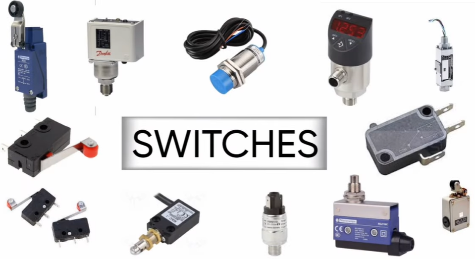
Data shows that after years of development, many outstanding companies have emerged in my country in the fields of switches, PA, WIFI FEM, filters and other subdivisions, and the global market share of RF front-end companies has reached more than 10%.

From a global perspective, the top five leading RF front-end companies have a combined market share of up to 80%, and there is still a lot of room for domestic substitution. Although there are many domestic start-ups pouring into the radio frequency track, there are still “partiality” situations.

For example, filter products are mostly concentrated in the mid- to low-end, and there is a lack of high-end products.

The materials, processes and packaging and testing technologies involved in RF front-end chips are not simple. How to achieve high-end breakthroughs in specific fields is still a big test for domestic RF companies.

With the technological advancement of 6G and WIFI7, as well as the popularization and promotion of UWB (ultra-wide) applications, future communication technology innovations will also bring new applications and new needs.

This “Communications and Radio Frequency Technology” forum mainly focuses on cutting-edge communications and radio frequency technologies, discusses the opportunities and challenges that emerging communications technologies bring to radio frequency technology, as well as the development of my country’s radio frequency front-end chip and module industry, and shares the latest application results. Promote my country’s radio frequency industry to advance into high-end fields.

“Innovation Release and Application Docking” Forum

China has become the world’s largest electronic application market, with chip demand ranking first in the world. In order to accelerate the docking and promotion of upstream and downstream applications, ICDIA will select 30 chips with the most market potential based on more than 1,000 domestic chip companies collected in the “China Chip Product Catalog” (formerly China Chip Compilation) and organize roadshow releases and application docking , assisting upstream and downstream collaboration.

Chip innovation supports and leads technological innovation. “Innovation Release and Application Docking” will invite major electronic equipment companies, R&D institutions, and system manufacturers to participate. It will also invite experts, scholars, business representatives, etc. to provide suggestions for accelerating the development of the domestic chip industry.

Four major exhibitions gathered at the same time

IC Application Expo “New”

In addition to the ICDIA Summit Forum and thematic forums, the IC Application Exhibition, the 11th Automotive Electronics Innovation Conference and Exhibition (AEIF), the 5th Automotive Chip Supply and Demand Matchmaking Conference, and the 12th Semiconductor Equipment Annual Conference and Semiconductor Equipment were held concurrently. The display of core components (CSEAC 2024) is also exciting.

IC Application Exhibition (IC Expo)

IC Expo is the first professional boutique exhibition dedicated to chip innovation, software, system solutions and product applications. The exhibition is divided into three major exhibition areas: [Innovative Chinese Chip], [Automotive Electronics], and [Black Technology Application], focusing on IC design technology, artificial intelligence, intelligent terminals, Internet of Things, smart transportation, in-vehicle entertainment, health technology, sports technology, and smart technology. New products, new technologies, new scenarios, and new applications such as home furnishings.

AEIF 2024

This year’s 11th AEIF will focus on the innovative development of the domestic and foreign automotive semiconductor industry and explore automotive electronics technology paths and market trends. The forum held at the same time focused on topics such as the development of intelligent connected vehicles, automotive chip system design innovation, and new energy vehicle innovation. The “Domestic Automotive Chip Reliability Grading Catalog (2024)” will also be released at the meeting, and there will also be an automotive chip supply and demand matchmaking meeting Promote the docking of automotive chip production and research, production and demand, and industry and finance.

From September 25th to 27th, 2024, we will gather in Wuxi to discuss the chip industry ecology and application development. We look forward to your arrival!

About ICDIA

The China Integrated Circuit Design Innovation Conference (ICDIA) focuses on the ecological construction of the IC industry chain and is committed to promoting the application of chips in automobiles, communications, and consumer electronics. It is China’s first boutique exhibition focusing on IC design innovation and system applications.

Previous conferences have focused on displaying new products, new technologies, and new applications, focusing on promoting innovative IC products and application solutions in the fields of automotive electronics, artificial intelligence, consumer electronics, industrial control, communications, and the Internet of Things.

The conference includes 1 thousand-person summit forum, 6 theme forums, and 1 IC application exhibition, displaying the TOP 100 best Chinese chips and innovative black technologies, and promoting new products, new technologies, and new applications.

IC design companies from across the country, supply chain procurement centers of various brands of electronic manufacturers, and R&D teams of major technology companies gathered together to share chip innovation results and future applications, and to take the pulse of new trends, trends, and trends in electronic technology.

Explore electronic component procurement quality control technology

Explore electronic component procurement quality control technology

Electronic component procurement quality control technology is a key link in ensuring the quality and reliability of electronic products.

With the rapid development of the electronics industry, the types and quantities of electronic components are increasing, and the requirements for quality control technology are becoming higher and higher.

This article will introduce the quality control technology of electronic component procurement in detail to provide comprehensive understanding and guidance.

Overview

Electronic component procurement quality control technology refers to the quality inspection, testing and control of purchased electronic components through a series of technologies and means to ensure that they meet design requirements and reliability standards. Quality control technology involves many aspects, including appearance inspection, performance testing, reliability and life evaluation of components.

Key elements

  1. Appearance inspection
    Appearance inspection is one of the most basic procurement quality control techniques. By inspecting the appearance dimensions, surface quality, markings and packaging, we can preliminarily judge whether the components meet the requirements. Appearance inspection is generally performed using visual or automatic inspection equipment.
  2. Performance testing
    Performance testing is an important means to evaluate the function and performance of components. Through testing, it can be determined whether the electrical parameters, frequency characteristics, temperature characteristics, etc. of the components meet the design requirements. Performance testing is generally performed using automatic testing equipment, and corresponding testing specifications and standards need to be formulated.
  3. Reliability and Lifetime Assessment
    Reliability and life assessment is a test of the long-term stability of components. The life and reliability of components are analyzed through accelerated aging tests, life tests, etc. This process needs to be carried out under specific environmental conditions, such as high temperature, low temperature, high humidity, etc., to accelerate the aging process of components.
  4. Quality assurance system
    Establishing a complete quality assurance system is the key to ensuring the quality of purchased components. The quality assurance system should include supplier selection and evaluation, procurement process control, inspection and testing, handling of non-conforming products, etc., and the system needs to be reviewed and updated regularly.
  5. Information management
    Adopting information management methods, such as establishing an electronic components database and using a procurement management system, can realize information sharing, process optimization and data statistics and analysis in the procurement process, and improve procurement efficiency and quality control levels.
Electronic Components Purchasing Website

Application and practice

In practical applications, electronic component procurement quality control technology should be selected and applied based on specific needs and actual conditions. The following are some common application scenarios and practical experiences:

  1. Supplier selection and evaluation: When selecting suppliers, a comprehensive evaluation of the supplier’s qualifications, quality assurance capabilities, product performance, etc. should be conducted. Supplier evaluation scales and other methods can be used for evaluation and scoring to ensure reliable supplier quality.
  2. Formulation of inspection and testing plans: Develop corresponding inspection and testing plans based on the type, specifications and usage requirements of components. The plan should include appearance inspection, performance testing, reliability and life evaluation, etc., and clarify the testing methods and qualification standards.
  3. Disposal of unqualified products: Unqualified components should be identified, isolated and processed. The processing method can be returned, exchanged or scrapped according to the actual situation, and the unqualified products need to be analyzed and the causes traced.
  4. Continuous improvement: By analyzing and summarizing quality problems that arise during the procurement process, we will identify the root causes and take corresponding improvement measures. At the same time, quality control technology is regularly reviewed and updated to adapt to changing market needs and technological developments.
  5. Personnel training and awareness raising: Strengthen the training and awareness raising of procurement personnel and quality inspection personnel, so that they can fully realize the importance of procurement quality control and improve quality awareness and operational skills.
  6. Preventive maintenance and upkeep: Perform regular preventive maintenance and upkeep on quality inspection equipment to ensure the normal operation and use of the equipment. At the same time, the maintenance and upkeep process should be recorded and tracked to ensure the reliability and stability of the equipment.
  7. Green and environmentally friendly procurement: Consider environmental protection factors during the procurement process, give priority to component suppliers and products that meet environmental standards and quality requirements, and promote the development of green and environmentally friendly procurement.
  8. Information management system application: Use the information management system to comprehensively manage the procurement process and realize functions such as information sharing, process optimization, and data statistics and analysis. Improve procurement efficiency and quality control levels through system automation and intelligent reminders.
  9. Supply chain collaboration: Strengthen communication and collaboration with suppliers to achieve supply chain synergy. Improve the reliability and stability of the supply chain through information sharing, real-time feedback and joint problem solving.
  10. International quality standards and certification: Establish corresponding quality control systems and quality assurance measures in accordance with international quality standards and certification requirements. Improve the international competitiveness and market share of products through the acquisition of international quality standards and certifications.

Electronic component procurement summary

Electronic component procurement for PCB circuits

Electronic component procurement quality control technology is an important means to ensure the quality and reliability of electronic products. In practical applications, the corresponding quality control technology should be selected and applied based on specific needs and actual conditions.

In the future, with the continuous development of the electronics industry, the types and performances of electronic components will become more diversified, and the requirements for quality control technology will also become higher and higher. Therefore, it is necessary to continuously update and improve the quality control technology system, improve quality control levels and technological innovation capabilities, to adapt to changing market demands and technological development.

At the same time, exchanges and cooperation with international advanced enterprises should be strengthened, and international advanced quality control technologies and experiences should be absorbed and used to promote the sustainable development and innovation progress of my country’s electronic component procurement quality control technology.

Wireless Modules Electronic Components Resistors Capacitors Transistors Connectors Chip IC Integrated Circuit

Frequently Asked Questions

What is electronic component procurement quality control technology?

Electronic component procurement quality control technology refers to the quality inspection, testing and control of purchased electronic components through a series of technologies and means to ensure that they meet design requirements and reliability standards.

What aspects does quality control technology include?

Quality control techniques include but are not limited to appearance inspection, performance testing, reliability and life evaluation, etc.

What is the purpose of visual inspection?

Appearance inspection is one of the most basic procurement quality control techniques. Through inspection of appearance dimensions, surface quality, marking and packaging, a preliminary judgment is made as to whether the components meet the requirements.

How is performance testing performed?

Performance testing is an important means to evaluate the function and performance of components. Through testing, it can be determined whether the electrical parameters, frequency characteristics, temperature characteristics, etc. of the components meet the design requirements. Performance testing is generally performed using automatic testing equipment, and corresponding testing specifications and standards need to be formulated.

What is the importance of reliability and lifetime assessment?

Reliability and life assessment is a test of the long-term stability of components. The life and reliability of components are analyzed through accelerated aging tests, life tests, etc. This process needs to be carried out under specific environmental conditions, such as high temperature, low temperature, high humidity, etc., to accelerate the aging process of components.

How to establish a quality assurance system?

Establishing a complete quality assurance system is the key to ensuring the quality of purchased components. The quality assurance system should include supplier selection and evaluation, procurement process control, inspection and testing, handling of non-conforming products, etc., and the system needs to be reviewed and updated regularly.

What are the practical applications of quality control techniques?

The application of quality control technology in practice includes supplier selection and evaluation, inspection and testing plan formulation, handling of non-conforming products, continuous improvement, personnel training and awareness raising, etc. In addition, preventive maintenance and upkeep, green and environmentally friendly procurement, information management system applications, supply chain collaboration, etc. are also important application directions.

Research on aging of plastic encapsulated microcircuit

Research on aging of plastic encapsulated microcircuit

The research on the aging of plastic-encapsulated microcircuits aims to explore the mechanism and rules of performance degradation of plastic-encapsulated microcircuits during long-term use, and provide theoretical support for extending the service life of microcircuits.

Introduction

In today’s highly automated electronics manufacturing world, the performance stability of microcircuits is critical. As one of the important forms, plastic microcircuit is widely used in various electronic devices.

However, plastic-encapsulated microcircuits may have potential early failure issues due to various factors during the manufacturing process.

Therefore, it is particularly important to age plastic-encapsulated microcircuits to detect and eliminate potential early failure factors in advance. This article will discuss in detail the principles, methods, technological progress and challenges of plastic microcircuit aging.

The principle of aging of plastic encapsulated microcircuit

The principle of aging of plastic encapsulated microcircuit

Aging refers to the process of accelerating the exposure of potential early failure factors by applying certain stress conditions after the electronic components are manufactured. For plastic-encapsulated microcircuits, aging usually includes temperature stress, electrical stress, etc. Through aging, potential early failure factors can be discovered and eliminated in advance, and the reliability and stability of microcircuit can be improved.

Methods for aging plastic microcircuits

  1. Temperature cycle aging: Temperature cycle aging is a commonly used aging method. In this method, plastic-encapsulated microcircuits are exposed to a range of high and low temperatures to simulate temperature changes in actual use. In this way, the adaptability of plastic-encapsulated microcircuits to temperature changes and potential thermal stress issues can be detected.
  2. Electric stress aging: Electric stress aging is to detect changes in the electrical properties of plastic-encapsulated microcircuits by applying a certain amount of electrical stress. This method can detect potential electrical problems in plastic microcircuits, such as electromigration, arcing, etc.
  3. Comprehensive aging: In addition to temperature cycle and electrical stress aging, comprehensive aging can also be carried out in combination with other stress conditions, such as mechanical stress, humidity, etc. Comprehensive aging can more comprehensively simulate the actual use environment and more accurately detect potential problems with plastic-encapsulated microcircuits.

Technological progress in plastic encapsulated microcircuit aging

With the continuous development of science and technology, the aging technology of plastic encapsulated microcircuit is also constantly improving. For example, the emergence of new testing equipment makes it possible to conduct high-precision electrical performance testing of plastic microcircuits; the development of new analysis tools can help engineers more accurately identify and locate problems in plastic microcircuits; in addition, artificial intelligence and Machine learning technology is also increasingly used in plastic microcircuit aging. They can help engineers analyze data more quickly, predict potential failure modes, and provide corresponding optimization suggestions.

Challenges and prospects of plastic microcircuit aging

Although plastic microcircuit aging technology has made great progress, it still faces some challenges. For example, how to more accurately simulate the aging conditions of the actual use environment, how to improve the efficiency of aging, and how to reduce the cost of aging, etc. In order to solve these problems, future research work can be carried out from the following aspects: first, in-depth study of the failure mechanism of plastic microcircuit to more accurately identify and locate potential problems; second, develop more efficient aging methods and equipment , to improve aging efficiency and reduce costs; finally, combine new technologies such as artificial intelligence and machine learning to develop an intelligent aging system to achieve automated aging and analysis.

Summarize

By aging the plastic-encapsulated microcircuit, its reliability and stability can be effectively improved. In order to carry out aging better, we need to continue to conduct in-depth research and explore new aging methods and equipment. In the future, with the continuous development of science and technology, we look forward to achieving more breakthroughs and innovations in the field of plastic microcircuit aging.

Frequently Asked Questions and Answers on Plastic Microcircuit Burning Research

What is plastic microcircuit aging?

Plastic microcircuit aging is a process that accelerates the exposure of potential early failure factors of microcircuits by simulating the stress conditions in the actual use environment.

What is the purpose of aging plastic microcircuits?

Answer: The main purpose of aging plastic microcircuits is to improve the reliability and stability of microcircuits and to discover and eliminate potential early failure factors in advance. Through aging, the risk of early product failure can be reduced and the quality and reliability of the product can be improved.

What are the common aging methods for plastic-encapsulated microcircuits?

Common plastic microcircuit aging methods include temperature cycle aging, electrical stress aging, and mechanical stress aging. These methods can test microcircuit performance and potential problems in different environments by applying different stress conditions.

What is the basic principle of plastic microcircuit aging?

The basic principle of aging plastic microcircuits is to accelerate the exposure of potential problems in microcircuits by applying certain stress conditions. These stress conditions can include temperature, electrical stress, mechanical stress, etc. to simulate the environmental conditions in actual use.

What are the principles and applications of temperature cycle aging?

Temperature cycle aging simulates the temperature changes in actual use by exposing the microcircuit to high and low temperatures. In this way, thermal performance and thermal stress issues of microcircuits can be detected, as well as their reliability and stability evaluated at different temperatures.

What are the principles and applications of electrical stress aging?

Electrical stress aging is to detect changes in the electrical performance of microcircuits by applying a certain amount of electrical stress. This method can detect potential electrical problems in microcircuits, such as electromigration, arcing, etc. Through electrical stress aging, the stability and reliability of microcircuit under different operating voltages and currents can be evaluated.

What are the current research status and development trends of plastic microcircuit aging?

Research on the aging of plastic microcircuits has made some progress, but it still faces some challenges and problems. Future development trends include the development of more efficient aging methods and equipment, in-depth research on the failure mechanisms of microcircuits, and the combination of new technologies such as artificial intelligence and machine learning to achieve more accurate and efficient aging analysis and evaluation. At the same time, as the requirements for reliability and stability of electronic products continue to increase, plastic microcircuit aging technology will be more widely used and valued.

Electronic component accelerated life testing technology

Electronic component accelerated life testing technology

Electronic component accelerated life testing technology is a test method that accelerates component failure by applying stress beyond the normal range, aiming to evaluate the life and reliability of components in a short time.

Introduction

With the rapid development of science and technology, electronic components are increasingly used in various fields, such as aerospace, medical equipment, communication systems, etc.

However, the reliability issues of electronic components have also become prominent. For some key components, their lifespan and reliability directly affect the stability and safety of the entire system.

Electronic component accelerated life testing technology

Therefore, how to conduct effective life tests and quickly evaluate the life and reliability of electronic components has become the focus of the industry. This article will conduct a detailed analysis and discussion of accelerated life testing technology for electronic components.

Basic concepts of accelerated life testing of electronic components

Accelerated Life Testing (ALT) of electronic components is a testing method that accelerates the failure of components by applying stress beyond the normal operating range, such as voltage, current, temperature, etc. Through accelerated life testing, the life and reliability of components can be evaluated in a short period of time, providing a basis for product design, production and quality control.

Test principle

The principle of accelerated life testing is based on the “stress-life” relationship. Under a certain stress, the life of electronic components shows a certain distribution pattern.

How to check NPN and PNP Transistor using Digital Multimeter in urdu/hindi

By applying stress beyond the normal operating range, the life of a component can be shortened and its failure accelerated. In this way, the life and reliability of components can be evaluated in a shorter period of time.

Experiment method

  1. Constant stress accelerated life test: During the test, the applied stress remains constant. This method is simple and easy to implement, but the disadvantage is that the test results may be significantly different from the failure mode under actual use conditions.
  2. Step stress accelerated life test: During the test, the stress gradually increases until it reaches the preset failure criterion. This method can more realistically simulate stress changes under actual use conditions, but the test cycle is longer.
  3. Sequential stress accelerated life test: During the test, the stress increases in a linear or non-linear manner. In this way, the life and reliability of components can be evaluated in a shorter period of time.
  4. Accelerated degradation test: By periodically applying accelerated stress loading to electronic components, observe their performance degradation and predict their life and reliability under normal stress. This method needs to be carried out with online monitoring equipment.
Implementation steps of accelerated life testing of electronic components

Implementation steps of accelerated life testing of electronic components

  1. Determine the purpose of the test: Make it clear whether the goal of the test is to evaluate the life and reliability of the components or to improve the design of the product.
  2. Select the test method: Select the appropriate accelerated life test method according to the actual situation.
  3. Determine the acceleration factor: Select the appropriate acceleration factor (such as voltage, current, temperature, etc.) based on the characteristics of the component and actual usage conditions.
  4. Develop a test plan: including the number of samples to be tested, loading methods, test methods, data records, etc.
  5. Carry out the test: Carry out the accelerated life test according to the test plan.
  6. Data processing and analysis: Process and analyze test data to evaluate the life and reliability of components.
  7. Conclusions and suggestions: Draw conclusions based on the test results and make suggestions for improving product design and production processes.

Limitations of accelerated life testing of electronic components

Although accelerated life testing can evaluate the life and reliability of components in a shorter period of time, there are still some limitations:

  1. Difficulty in selecting acceleration factors: Different acceleration factors may have different effects on the failure modes and mechanisms of components. Selecting an appropriate acceleration factor is a challenging task.
  2. Extrapolation of test results: Since the accelerated life test is conducted under stress beyond the normal operating range, the reliability of the extrapolation of the test results to actual use conditions needs to be handled with caution.
  3. Insufficient representativeness of samples: Since accelerated life testing requires a large number of samples and time, it is sometimes difficult to ensure the representativeness of the samples, which may have a certain impact on the test results.
  4. High cost: Accelerated life testing requires professional equipment and manpower investment, as well as a large number of samples and time, so the cost is high.

Summary and prospects of accelerated life testing technology for electronic components

Accelerated life testing technology for electronic components is an important reliability assessment method that can quickly evaluate the life and reliability of components and provide a basis for product design, production and quality control. Although there are certain limitations, this technology still has high practical value in some specific situations.

In the future, with the continuous advancement of technology and the increase in application demand, the accelerated life testing technology of electronic components is expected to be further developed and improved. For example, the accuracy and reliability of this technology can be further improved by improving the acceleration factor selection method, optimizing the test plan, and improving test efficiency.

electronic components factory

At the same time, with the development of artificial intelligence and machine learning technologies, these technologies can be used to conduct in-depth analysis and mining of accelerated life test data to gain a more comprehensive understanding of the performance and reliability of electronic components. In addition, other evaluation methods such as physical analysis and chemical analysis can be combined to further reveal the mechanism and causes of electronic component failure, and provide more targeted suggestions and solutions for its reliability design and optimization.

FAQs

What is accelerated life testing of electronic components?

Accelerated life testing of electronic components is a testing method that accelerates component failure by applying stress beyond the normal operating range, such as voltage, current, temperature, etc. Through accelerated life testing, the life and reliability of components can be evaluated in a short period of time, providing a basis for product design, production and quality control.

What is the purpose of accelerated life testing of electronic components?

The purpose of accelerated life testing of electronic components is to evaluate the life and reliability of components and improve product design. Through accelerated life testing, weak links and reliability issues of components can be quickly determined, providing a basis for product optimization and improvement.

How to choose the appropriate acceleration factor?

Choosing the appropriate acceleration factor is the key to accelerated life testing of electronic components. Common acceleration factors include voltage, current, temperature, etc. When selecting an acceleration factor, its impact on component failure modes and mechanisms, as well as stress levels under actual use conditions, should be considered. At the same time, the selection of acceleration factors should also consider test cost and operability.

How to determine the number of test samples?

The number of test samples should be determined based on factors such as test purpose, test time and resources. Too few samples may lead to inaccurate results, while too many samples may increase the cost and time of the test. It is recommended to make a reasonable selection based on the actual situation and consider the representativeness and difference of the sample.

How to deal with accelerated life test data?

Accelerated life test data should be statistically analyzed and processed to evaluate component life and reliability. Common statistical analysis methods include probability distribution fitting, life test data analysis, reliability assessment, etc. Through data analysis, the life distribution, failure modes and reliability indicators of components can be determined.

How to interpret accelerated life test results?

Accelerated life test results should be interpreted based on actual conditions. Test results can provide information on the life and reliability of components, but it is necessary to pay attention to the difference between test conditions and actual use conditions. In addition, abnormal results or results that do not match expectations require in-depth analysis and explanation.

How are accelerated life test results applied?

The application of accelerated life test results should be based on specific needs. The test results can be used to improve product design, production and quality control, and improve the reliability and stability of components. At the same time, accelerated life test results can also be used to evaluate the effectiveness and accuracy of component life prediction models and reliability assessment methods.

What is a Semiconductor PCB (Printed Circuit Board)?

What is a Semiconductor PCB (Printed Circuit Board)

Semiconductor PCB uses semiconductor as the base material, on which other electronic components and semiconductor devices are connected.

Most semiconductor PCBs are relatively small compared to regular PCBs, making them ideal for small appliances such as smart watches.

Semiconductor PCB is also called semiconductor printed circuit board.

Difference between PCB and Semiconductor

Difference between PCB and Semiconductor

PCB (Printed Circuit Board) and semiconductors have their own unique roles and functions in the electronics industry.

First, a semiconductor is a raw material that can control electric current, such as silicon and germanium. Semiconductors are the basic materials for making electronic components, such as transistors, diodes, integrated circuits, etc. These electronic components can be used to control electric current, amplify and process electronic signals.

PCB is a plate made of conductive material on which some circuits and other component structures are formed to realize electrical connections between electronic components. Unlike semiconductors, PCB is not a raw material, but a basic component that connects various electronic components. The design and manufacturing of PCB is crucial to the realization of electronic products. It not only allows various electronic components to be connected, but also fixes the position and connection method of components in circuit design.

Although PCBs and semiconductors have obvious differences in definition and function, they complement each other in electronic products. Semiconductor devices such as transistors are widely used in PCBs. These devices are supported and connected through PCB boards to form a complete circuit.

Overall, PCBs and semiconductors each have their own unique role in the electronics industry. Semiconductors, as basic materials, are mainly used to make various electronic components; PCB, as a basic component, is mainly used to realize electrical connections between electronic components. In practical applications, the two often need to cooperate with each other to realize the functions of electronic products.

Semiconductor PCB materials

Semiconductor PCB materials

Semiconductor PCB materials mainly include FR-4, PP semi-solid sheets, Core core boards, etc. Among them, the Core board is composed of copper foil, solid resin material and glass fiber, and has a certain hardness and thickness. The PP semi-solid sheet is composed of semi-solid resin material and glass fiber, and is mainly used to fill the adhesive material and insulating material of the inner conductive pattern of multi-layer printed boards.

In addition, there are PCBs using silicon carbide materials, which are suitable for high-temperature circuit boards because of their high thermal conductivity. There are also PCBs using FR-4 material, which has good insulation properties, mechanical strength and thermal stability.

Semiconductor PCB layout

Semiconductor PCB Design

The process of semiconductor PCB (printed circuit board) design includes the following steps:

Determine design requirements

According to specific application requirements, clarify the circuit’s functions, performance indicators, size, cost and other requirements.

Select appropriate substrates and components

According to design requirements, select appropriate substrates and components, such as integrated circuits, transistors, resistors, capacitors, etc.

Circuit design

According to the design requirements, use circuit design software to design circuit schematics and PCB layout. In the design, factors such as signal transmission, power distribution, component layout, and wiring direction need to be considered.

Determine PCB specifications and number of layers

Determine PCB specifications and number of layers according to the complexity and size requirements of the circuit. Multilayer PCBs are beneficial to reducing size and cost, but will increase the difficulty of design and manufacturing.

Wiring design

According to the circuit design, use wiring tools to design PCB wiring. In the wiring design, factors such as the direction, width, and spacing of the wiring need to be considered to ensure the normal operation of the circuit.

Verification and optimization

After completing the wiring design, circuit verification and optimization need to be performed to ensure the correctness and reliability of the design. At the same time, the PCB also needs to be optimized to improve its manufacturability and reliability.

Board making

Submit the designed PCB files to a professional board making factory for production. During the board making process, it is necessary to ensure the quality and accuracy of the board making to ensure the final circuit performance.

Testing and verification

After completing the board manufacturing, the PCB needs to be tested and verified to ensure that its performance meets the design requirements. If problems are found, corresponding modifications and optimizations need to be made.

Document organization and archiving

Finally, organize the entire design process into documents and archive them for subsequent design reference and use.

During the entire semiconductor PCB design process, it is necessary to comprehensively consider factors such as circuit performance, size, cost, etc., select appropriate substrates and components, and optimize circuit design and wiring design to ensure final circuit performance and reliability. At the same time, attention must be paid to complying with relevant design specifications and standards to ensure the legality and compliance of the design.

Semiconductor PCB Layout

In semiconductor PCB layout, the following factors need to be considered:

Component layout

Follow the layout principle of “large first, then small, difficult first, easy later”, that is, important unit circuits and core components should be laid out first.

At the same time, refer to the schematic block diagram and arrange the main components according to the main signal flow pattern of the single board.

In addition, the arrangement of components should be convenient for debugging and maintenance, that is, large components should not be placed around small components, and there should be enough space around components that need to be debugged.

Circuit board size

Determine the optimal shape and size of the circuit board based on the function and complexity of the circuit board, as well as the actual number of components that need to be carried.

Process requirements

According to the requirements of the production process, determine the layout and wiring method of the PCB. For example, in a multi-layer PCB, the signal routing and connection methods between the layers, as well as the distribution of power and ground, need to be considered.

Thermal design

Thermal design needs to be considered during layout. According to factors such as the heat generation and heat dissipation conditions of the components, the locations of the components should be reasonably arranged and appropriate heat dissipation measures should be taken.

Electromagnetic compatibility

Electromagnetic compatibility needs to be considered during layout, and the location and routing of components should be reasonably arranged to reduce electromagnetic interference and noise.

Reliability

Reliability needs to be considered during layout and appropriate measures should be taken to improve the reliability and stability of the circuit board. For example, redundant design of key components, adding power filters, etc.

In short, semiconductor PCB layout needs to consider multiple factors to ensure that the circuit board has good performance, reliability and stability. At the same time, layout solutions need to be continuously optimized and improved to improve production efficiency and quality.

Semiconductor PCB functional characteristics

Semiconductor PCB (Printed Circuit Board) is a circuit board with semiconductor devices. Its functional characteristics mainly include the following aspects:

High-density integration

Semiconductor PCB uses high-density wiring technology, which can integrate a large number of electronic components and wires into one, and has the characteristics of high density and miniaturization.

High reliability

Semiconductor PCB uses high-quality substrates and advanced process technology, has good electrical performance and stability, and can ensure high-reliability circuit connections and signal transmission.

High efficiency

The high-density integration and short-line connection design of semiconductor PCB can reduce the delay and loss of signal transmission and improve the working efficiency of the circuit.

Good heat dissipation performance

The semiconductor devices on the semiconductor PCB will generate heat, and the base material of the PCB has good thermal conductivity, which can quickly conduct the heat out and ensure the normal operating temperature of the electronic components.

Easy to maintain and upgrade

The electronic components and circuits on the semiconductor PCB are standardized and easy to maintain and upgrade. At the same time, the design and manufacturing process of PCB also make it have good repairability and replaceability.

Diversified application fields

Semiconductor PCB has a wide range of application fields, including communications, computers, consumer electronics, automotive electronics, etc., which can meet the needs of different fields.

In general, semiconductor PCB has the characteristics of high-density integration, high reliability, high efficiency, good heat dissipation performance, easy maintenance and upgrade, and diversified application fields. It is one of the indispensable and important components in modern electronic equipment. .

Development History of Semiconductor PCB

Development History of Semiconductor PCB

The development history of PCB (Printed Circuit Board) can be traced back to the early 20th century, and the emergence and application of semiconductors occurred decades after that. The following is the development history of semiconductor PCB:

Early exploration stage (1900-1940s)

In the early 20th century, people began to explore circuit connections in electronic devices. At this stage, any electronic device contains many wires, which not only get tangled together and take up a lot of space, but short circuits are not uncommon. German inventor Albert Hansen pioneered the concept of using “wires” for telephone switching systems in 1903 and conceived the idea of metal foil being used to cut line conductors. These early explorations laid the foundation for later PCB inventions.

PCB Enlightenment Stage (1920s-1940s)

In the 1920s, American inventor Charles Ducas printed circuit patterns on insulating substrates, and then used electroplating to create conductors for wiring. It is a symbol of opening up modern PCB technology. In 1936, Paul Eisler published foil technology in the UK. He used a printed circuit board in a radio device, which is considered the world’s first true PCB. In the same year, Japan’s Miyamoto Kinosuke successfully applied for a patent for the spray-on wiring method “Micro Blowing Wiring Method (Patent No. 119384)”. By 1943, Americans used this technology extensively in military radios.

Rapid development stage (1950s-1980s)

With the recovery of the post-war economy and the rapid development of the electronics industry, PCB manufacturing technology and semiconductor technology began to develop rapidly. In 1953, Motorola developed a double-sided panel with electroplated through-holes and later applied it to multi-layer circuit boards.

By 1960, V. Dahlgreen used metal foil film with printed circuits attached to plastic to create a flexible printed circuit board. In 1961, the Hazeltine Corporation in the United States made reference to the electroplating through-hole method and produced multilayer boards.

Since then, with the continuous advancement of technology and the expansion of the market, PCB and semiconductors have gradually become an important part of the electronics industry.

Modern application stage (1990s to present)

As electronic products continue to become miniaturized and intelligent, the design and manufacturing technology of PCB and semiconductors also continue to advance. In 1995 and 1996, Panasonic and Toshiba developed ALIVH and B2IT build-up printed circuit boards respectively.

After entering the 21st century, the application fields of PCB and semiconductors have further expanded, involving communications, computers, consumer electronics, automotive electronics, medical electronics and other fields.

At the same time, the application of emerging technologies such as green manufacturing and smart manufacturing also provides new opportunities for the sustainable development of PCBs and semiconductors.

In general, the development of PCB and semiconductors complements each other. As the support and connection basis of electronic products, PCB provides a reliable installation platform and circuit channel for semiconductor devices; and the continuous expansion of semiconductor performance and application fields also provides PCB with more functions and higher integration. In the future, with the continuous development of technology, PCB and semiconductors will continue to drive the development and innovation of the electronics industry.

What is a semiconductor pcb used for

Semiconductor PCBs are widely used in many fields. Here are some common uses:

  1. Electronic equipment manufacturing: PCB is an important part of electronic equipment manufacturing. It is used to connect electronic components together to achieve circuit control and communication.
  2. Automobile industry: In the automobile industry, PCB is widely used in control systems, such as engine control, brake system control, etc.
  3. Military industry: In the military industry, PCB is used in various military equipment, such as radars, missile control systems, etc.
  4. Medical equipment: Many medical equipment, such as heart monitors, medical crutches, etc., use PCB technology to achieve more efficient signal control.
  5. Consumer electronics: PCB boards are widely used in the manufacturing of consumer electronics such as mobile phones, laptops, tablets, etc.

In short, semiconductor PCB has a wide range of uses and plays an important role in promoting the development of modern industry.

Application of semiconductor PCB in medical field

Application of semiconductor PCB in medical field

In the medical field, the application of semiconductor PCB is mainly reflected in the manufacturing of medical equipment. Medical equipment requires high-precision and high-reliability circuit boards to support its operation, and semiconductor PCBs precisely meet these requirements.

For example, in medical imaging equipment, such as CT, MRI and X-ray machines, PCBs are used to receive and transmit image signals to ensure the normal operation of the equipment and the accuracy of diagnosis. In addition, in monitoring equipment, such as electrocardiographs, blood pressure monitors, and blood glucose meters, PCBs also play a key role in collecting, processing, and transmitting physiological data.

In medical devices, such as pacemakers, implantable defibrillators, and neurostimulators, PCBs are an integral part. These devices need to be implanted into the human body for a long time, so the PCB is required to have extremely high reliability and stability.

In general, semiconductor PCBs are widely used in the medical field and play an important role in improving the performance and reliability of medical equipment and ensuring patient safety.

Application of semiconductor PCB in automotive field

In the automotive field, the application of semiconductor PCB is equally important. Here are some specific examples:

Engine control unit (ECU)

ECU is the key control center of the automobile engine. It is responsible for receiving various sensor signals and issuing instructions to control the work of the engine. PCB plays a core role in the ECU and is used to implement signal processing and transmission.

Vehicle infotainment systems

These systems include center console displays, audio equipment, navigation systems, etc. They require complex PCB boards to support various functions.

Air conditioning control module

By controlling parameters such as fan speed and temperature, the PCB maintains a comfortable temperature in the car.

Safety systems

Such as the airbag control module, which is responsible for monitoring the situation and inflating when needed to protect passengers in the event of a collision.

Anti-lock braking system (ABS)

ABS prevents wheels from locking by monitoring the speed of the wheels and adjusting the braking force. PCB is also used in this.

Sensor module: includes various sensors, such as temperature sensor, pressure sensor, light sensor, etc., which are used to monitor vehicle status and transmit data to the on-board computer.

Electric seat control module

This module controls the adjustment of the electric seat, including seat height, front and rear, tilt, etc.

Lighting control module

This module controls the lighting system inside and outside the car, including headlights, position lights, interior lighting, etc.

Body control module

This module is responsible for monitoring the status of the body, such as door status, window status, etc., and executing corresponding control actions.

Charging control module

For electric vehicles, this module is responsible for charging management and protection of the battery.

Driving assistance systems

Such as autonomous driving, reversing imaging, automatic parking, etc. These systems require complex electronic control and sensor support, and PCB is the key component to achieve these functions.

The above are some applications of semiconductor PCBs in the automotive field.

What is a Semiconductor PCB vs PCB

What is a Semiconductor PCB vs PCB

PCB (printed circuit board) and semiconductor PCB have their own unique roles in the electronics industry.

PCB is a plate made of conductive material on which some circuits and other components are formed to realize electrical connections between electronic components. It is the support body of electronic components and the carrier of electrical connections between electronic components, providing an indispensable foundation for the realization of electronic products. In addition, it not only allows various electronic components to be connected, but also can fix the position and connection method of components in circuit design.

Semiconductor PCB uses an empty PCB board to undergo processes such as SMT patching, DIP plug-in and testing to form a finished product, referred to as PCBA for short. It installs semiconductor devices on a PCB to form a complete circuit. Compared with PCB, semiconductor PCB goes one step further. It implements more electronic functions by installing various semiconductor devices, such as integrated circuits, transistors, diodes, etc., on the PCB.

Therefore, there are obvious differences in definition and function between PCB and semiconductor PCB. PCB is a basic electronic component, mainly used to support and connect electronic components; while semiconductor PCB further integrates semiconductor devices on the basis of PCB to achieve more complex electronic functions. In practical applications, the two often need to cooperate with each other to achieve the best performance of electronic products.

In general, PCB and semiconductor PCB each have their own unique role in the electronics industry. Although semiconductor PCBs are more complex in function, PCBs also play an indispensable role in electronic products as basic components. In practical applications, it is very important to choose the appropriate circuit board type according to different needs.

Which is more powerful, semiconductor or PCB?

Semiconductor PCB circuit diagram - Which is more powerful, semiconductor or PCB?

Semiconductors and PCBs each play an important role in the electronics industry and have different advantages and characteristics, so they cannot be compared simply.

Semiconductors are core components of electronic products, capable of controlling electrical current to achieve various electronic functions. Semiconductors are widely used in the electronics industry, including integrated circuits, transistors, diodes, etc. With the development of technology, the performance of semiconductors continues to improve, and the application fields continue to expand.

PCB is the support and connection basis of electronic products. It can connect various electronic components to form a complete circuit. PCB design and manufacturing are critical to the performance and stability of electronic products. In the R&D and production of electronic products, the design and manufacturing of PCBs need to work closely with the design and manufacturing of semiconductors to ensure the correctness and reliability of the circuits.

Therefore, both semiconductors and PCBs are important parts of the electronics industry, each with its own unique advantages and characteristics. In practical applications, the two often need to cooperate with each other to achieve the best performance of electronic products. Today, with the rapid development of technology, the performance and application fields of semiconductors are constantly expanding, and PCB design and manufacturing technology are also constantly improving, both of which are driving the development of the electronics industry.

PCB or semiconductor PCB, which one is more expensive?

In terms of price, semiconductor PCB and PCB each have their own characteristics and factors that affect their cost and price.

Generally speaking, PCB design and manufacturing are relatively simple, so the price is relatively low. Semiconductor PCB further integrates semiconductor devices on the basis of PCB. Its manufacturing cost is relatively high, so the price is also relatively high.

In addition, the prices of PCBs and semiconductor PCBs are also affected by factors such as different types, specifications, quality and workmanship. For example, high-density interconnect (HDI) PCB has the characteristics of high density, high performance and miniaturization, and its manufacturing cost and price are relatively high, while simple FR4 PCB is relatively low. In addition, different production scales and market demands will also affect prices.

Therefore, it is impossible to simply compare whether PCB or semiconductor PCB is more expensive. Different factors and specific situations need to be considered comprehensively. When choosing a circuit board, you need to weigh the actual needs and budget to choose the most suitable circuit board type.

Semiconductor PCB FAQs

What is PCB?

PCB (Printed Circuit Board), that is, printed circuit board, is the support for electronic components and the connection basis for electronic circuits.

What is a semiconductor PCB?

Semiconductor PCB is based on ordinary PCB and integrates semiconductor devices, such as integrated circuits, transistors, diodes, etc., to form a circuit board with specific functions.

What are the characteristics of semiconductor PCB?

The characteristics of semiconductor PCB include high-density integration, high reliability, high efficiency, good heat dissipation performance, easy maintenance and upgrade, and diverse application fields.

What are the application fields of semiconductor PCB?

Semiconductor PCB is widely used in communications, computers, consumer electronics, automotive electronics and other fields, and is an indispensable and important component in modern electronic equipment.

How to solve PCB short circuit problem?

PCB short circuit problems may be caused by improper soldering pad design, improper part orientation design, automatic plug-in bent feet, etc. Solutions include modifying the pad design, part orientation, or modifying the automatic plug-in bending feet.

How to avoid PCB corrosion pitfalls?

To avoid PCB corrosion traps, the angle between leads should be minimized to avoid sharp angles. At the same time, the use of modern manufacturing processes such as photosensitive etching solutions can also greatly reduce the formation of corrosion traps.

How to solve the tombstone device problem?

Tombstone device problems are often caused by asymmetric wiring patterns that spread heat unevenly across the device pads. Solutions include optimizing routing patterns so that heat spreads evenly across the device pads.

How to solve layout problems?

Layout is an important part of PCB design. Reasonable layout can improve circuit performance and reduce costs. Solutions include laying out the core components of each functional circuit as the center. The components should be arranged evenly, neatly and compactly on the PCB, minimizing and shortening the leads and connections between components, and arranging each component according to the flow of the circuit. The location of functional circuit units, etc.

How to ensure the reliability of PCB?

To ensure the reliability of PCB, we need to start from many aspects, including selecting appropriate substrates and components, optimizing design, improving process accuracy, strengthening quality management, etc. In addition, regular maintenance and inspection are also important measures to ensure the reliability of PCB.

Research on heat dissipation methods of electronic components

Research on heat dissipation methods of electronic components

Research on heat dissipation methods of electronic components is a key technology to ensure the stable operation of equipment, aiming to improve the reliability and service life of electronic equipment.

With the continuous development of science and technology, electronic equipment is used more and more widely.

As an important part of electronic equipment, the performance and reliability of electronic components are crucial to the operation of the entire equipment.

However, since electronic components generate a large amount of heat during operation, if the heat cannot be effectively dissipated and controlled, it will lead to component performance degradation, damage and even safety issues.

Therefore, research on heat dissipation methods of electronic components is of great significance for improving the performance and reliability of electronic equipment.

What is heat dissipation in electronics

The heat dissipation of electronic devices is to control the operating temperature of electronic devices to ensure their working temperature and safety. Since electronic components generate heat during operation, when the heat accumulates to a certain extent, the performance of the electronic components will be reduced or even damaged. Therefore, heat dissipation is one of the important measures to ensure the reliable operation of electronic equipment.

The main purpose of heat dissipation is to effectively dissipate the heat generated by electronic components to the surrounding environment to keep the temperature of the electronic components within the allowable range. The main methods of heat dissipation include natural heat dissipation, forced heat dissipation, liquid heat dissipation, heat pipe heat dissipation, etc. Among them, natural heat dissipation refers to using natural convection to dissipate heat to the surrounding environment; forced heat dissipation refers to dissipating heat to the surrounding environment through forced means such as fans; liquid heat dissipation refers to using liquid coolant to take away heat; heat pipe heat dissipation is Refers to the use of heat pipes to transfer heat to a distant place and then dissipate it.

In electronic components, a heat sink is a device used to absorb, conduct and dissipate the heat generated by electronic components. The main function of the radiator is to prevent electronic components from overheating, prevent component damage, and extend their service life. Radiators can be classified according to material, form and function.

In short, the heat dissipation of electronic devices is one of the important measures to ensure the reliable operation of electronic equipment. It is necessary to choose the appropriate heat dissipation method and radiator according to the actual situation to effectively control the temperature of electronic components.

The necessity of heat dissipation for electronic components

During the working process of electronic components, a large amount of heat will be generated due to the passage of current and the resistance of the component itself.

If this heat cannot be dissipated in time, it will cause the component temperature to rise, thus affecting its performance and reliability.

Under long-term high temperature working environment, electronic components may fail, be damaged, etc., shortening their service life. Therefore, in order to ensure that electronic components can work normally and stably, effective heat dissipation measures must be taken.

Main methods of heat dissipation for electronic components

Main methods of heat dissipation for electronic components

What is a Heat Sink?

Natural heat dissipation

Natural heat dissipation refers to the transfer of heat through air convection or radiation without the use of any external auxiliary equipment.

For some electronic components with low power consumption and low heat generation, natural heat dissipation can be used. For example, install components on a well-ventilated heat sink and use natural convection to remove heat.

Forced heat dissipation

Forced heat dissipation refers to the forced removal of heat through external devices. Commonly used forced cooling methods include cooling fans, heat sinks, etc. The cooling fan can take away the heat through the high-speed rotating fan blades, and the heat sink can use the thermal conductivity of metal to transfer the heat to other parts.

For some electronic components that generate large amounts of heat and need to be quickly dissipated, forced heat dissipation can be used. For example, installing a cooling fan and heat sink on the computer CPU can quickly take away the heat generated by the CPU.

Electronic component heat dissipation

Liquid cooling

Liquid cooling refers to the use of liquid media to transfer heat. Liquid cooling has the advantages of high heat transfer efficiency and good heat dissipation effect, but it also requires relatively complex pipelines and sealing structures.

For some electronic components with high power consumption and high heat generation, liquid cooling can be used to dissipate heat. For example, in large computers or high-power electronic equipment, liquid cooling can be used to remove heat.

Heat pipe heat dissipation

The heat pipe is an efficient heat transfer element. It uses the flow circulation of liquid under capillary action, absorbs heat at the heating end, evaporates, and then condenses at the cooling end to release heat.

heat dissipation calculation for electrical equipment

Heat pipes have the characteristics of extremely high thermal conductivity, excellent isothermal properties, variability of heat flow density, and reversibility of heat flow direction, and can effectively solve many difficult heat transfer problems.

The use of heat pipe cooling technology in electronic equipment can greatly improve the reliability and service life of the equipment.

Cooling fan

The high-speed rotation of the cooling fan generates a strong air flow and quickly takes away the heat. This method is common in small devices, such as laptops, small servers, etc.

Heat sink

Heat sink is a widely used and effective way of heat dissipation. It uses materials with good thermal conductivity such as metal to transfer the heat generated by components to the heat sink, and then dissipates the heat into the air through the heat sink. Common heat sinks include aluminum and copper.

Heat dissipation methods

Heat pipe technology

Heat pipe technology is an efficient heat transfer technology that uses the evaporation and condensation phase change mechanism inside the heat pipe to quickly transfer heat to the condensation end of the heat pipe, and then dissipates the heat through heat sinks and other methods. Heat pipe technology has the advantages of high heat transfer efficiency and high reliability, and is widely used in electronic equipment.

Liquid cooling

Liquid cooling is an efficient heat dissipation method that quickly removes heat through direct contact between liquid and electronic components. Liquid cooling can be divided into two methods: direct cooling and indirect cooling.

Direct cooling is mainly used in high-power density equipment, such as large servers, data centers, etc.; indirect cooling uses an intermediate media system, using liquid modules, thermal conductivity modules, etc. Devices conduct heat transfer in electronic components.

Heat pipe array

Heat pipe array is a large-scale heat dissipation method. Multiple heat pipes are combined and arranged to form a large-area radiator.

It is suitable for high-power equipment such as large servers and data centers. The heat pipe array has the advantages of large heat dissipation area and high heat transfer efficiency, and can effectively solve the heat dissipation problem in high-power equipment.

Electronic component cooling products

In general, there are many methods of forced heat dissipation, and the appropriate heat dissipation method needs to be selected according to the actual application scenario and needs. Factors such as power consumption, heat generation, working environment, cost and reliability need to be considered when selecting.

Principles for selecting heat dissipation methods for electronic components

The choice of cooling method depends on the specific application scenario and needs. When choosing, you need to consider the following factors:

Power consumption and heat generation

Choose the appropriate heat dissipation method according to the power consumption and heat generation of electronic components. Components with low power consumption and low heat generation can choose natural heat dissipation or simple forced heat dissipation; components with high power consumption and large heat dissipation need to choose efficient heat dissipation methods such as forced heat dissipation or liquid cooling.

Working environment

Choose the appropriate heat dissipation method according to the working environment of the equipment. In harsh environments (such as high temperature, high humidity, vibration, etc.), you need to choose more reliable heat dissipation methods, such as liquid cooling or heat pipe heat dissipation.

Cost and reliability

On the premise of meeting performance and reliability requirements, lower-cost heat dissipation methods should be selected as much as possible. At the same time, considering the long-term use and maintenance of the equipment, it is also necessary to choose a more reliable heat dissipation method.

Compatibility and maintainability

When selecting a cooling method, you also need to consider its compatibility and maintainability with other parts of the device. It should not have a negative impact on other parts and should be easy to maintain and replace.

Future development trends of heat dissipation technology for electronic components

With the continuous development of science and technology, the heat dissipation technology of electronic components is also constantly improving and improving.

Principles for selecting heat dissipation methods for electronic components

In the future, the heat dissipation technology of electronic components will develop in a more efficient, reliable, and environmentally friendly direction. At the same time, with the continuous emergence of new materials and new processes, it will also bring more possibilities to the heat dissipation technology of electronic components.

For example, new materials such as nanomaterials and graphene have extremely high thermal conductivity and mechanical strength and can be used to make more efficient radiators and heat pipes; new thermal interface materials can reduce thermal resistance and improve thermal conduction efficiency; and intelligent control Technology can automatically adjust the operating status of the cooling system according to the operating status of the equipment to achieve more intelligent management.

Electronic component cooling solutions

In short, the heat dissipation technology of electronic components is one of the important means to ensure the performance and reliability of electronic equipment.

In order to adapt to the evolving needs of electronic equipment, we need to continue to conduct in-depth research and practice new heat dissipation technologies to promote the development and progress of the electronics industry.

Frequently Asked Questions and Answers on Heat Dissipation Methods for Electronic Components

How to dissipate heat from high-heat devices?

There are many ways to dissipate heat for high-heat devices, including natural heat dissipation, forced heat dissipation, and liquid cooling. Among them, forced heat dissipation can be achieved through cooling fans, heat sinks, heat pipes, etc. For a small number of devices with low heat dissipation, natural heat dissipation can be used, but for devices with large heat dissipation, efficient heat dissipation methods such as forced heat dissipation or liquid cooling are required.

What is a high heat generating device?

High heat-generating devices refer to electronic components that generate a large amount of heat during operation. Since these components generate a lot of heat, if the heat is not dissipated in time, the temperature of the components will rise, affecting their performance and reliability.

How to choose the appropriate cooling method?

Choosing the right cooling method requires considering multiple factors, including power consumption and heat generation, working environment, cost and reliability. For components with low power consumption and low heat dissipation, you can choose natural heat dissipation or simple forced heat dissipation; for components with high power consumption and high heat dissipation, you need to choose efficient heat dissipation methods such as forced heat dissipation or liquid cooling. At the same time, factors such as the working environment, cost, and reliability of the equipment also need to be considered to select an appropriate heat dissipation method.

What should I pay attention to when using a radiator?

When using a radiator, you need to pay attention to the following points: First, make sure that the radiator is in close contact with high-heating components to maximize heat transfer; second, check the integrity of the radiator regularly, and replace it in time if it is damaged; Finally, keep the working environment clean to avoid dust and debris from affecting the heat dissipation effect.

What are the advantages of heat pipe cooling?

Heat pipe heat dissipation has the advantages of high heat transfer efficiency, excellent isothermal property, heat flow density variability, heat flow direction reversibility, etc., and can effectively solve many difficult heat transfer problems. The use of heat pipe cooling technology in electronic equipment can greatly improve the reliability and service life of the equipment.

What voltage is Vces

What voltage is Vces

The Vces voltage parameter is an important parameter of the triode, which reflects the operating characteristics of the triode in the saturated state.

Research on vces voltage parameters

The study of Vces voltage parameters can help us better understand the working principle and performance of triodes, so as to better select and use triodes when designing circuits.

Definition of Vces voltage parameters

Vces refers to the voltage between the collector and emitter when the triode is working in saturation state. During the operation of the transistor, when the base current is large enough, the collector current will no longer increase with the increase of the base current, and at this time the transistor enters a saturated state. In the saturated state, the voltage difference between the collector and emitter is Vces.

The meaning of Vces voltage parameters

The Vces voltage parameter has an important impact on the operating performance and service life of the triode. In circuit design, if the selected Vces is too small, the transistor will heat up seriously during operation, or even burn out; if the Vces selected is too large, the transistor will be unstable or even unable to work normally.

The meaning of Vces voltage parameters  -  Basic Electricity - What is voltage?

Therefore, the correct selection and use of Vces voltage parameters is crucial to ensure the operating stability of the transistor and extend its service life.

Factors affecting the Vces voltage parameters

The Vces voltage parameter is affected by many factors, including the material, structure, process, temperature, etc. of the transistor. Among them, temperature is one of the important factors affecting the Vces voltage parameters.

As the temperature increases, the Vces value will decrease. This is mainly because the increase in temperature will cause the carrier mobility of the semiconductor material to increase, which will increase the collector current and ultimately cause the Vces value to decrease.

Therefore, transistors used in high-temperature environments need to choose models with larger Vces values.

How to select and use Vces voltage parameters

  1. Choose an appropriate Vces value based on circuit requirements: When designing a circuit, you need to select an appropriate Vces value based on specific requirements. If the circuit works in a high temperature environment, you need to choose a model with a larger Vces value; if the circuit works in a low temperature environment, you can choose a model with a smaller Vces value.
  2. Consider the packaging form of the triode: Different packaging forms will affect the heat dissipation performance of the triode, and thus affect its Vces value. Therefore, when selecting a transistor, you need to consider the impact of its packaging form on heat dissipation to select an appropriate Vces value.
  3. Pay attention to the safe working area during use: When using the triode, you need to pay attention to its safe working area. If the working point is set improperly, it may cause the transistor to work in the cut-off area or saturation area, thus affecting its normal operation. Therefore, it is necessary to set the working point reasonably during use to prevent the triode from working in an unsafe working area.
  4. Pay attention to the heat dissipation problem of the triode: Since the triode will generate heat during operation, if the heat cannot be dissipated in time, it will cause the temperature of the triode to rise, thus affecting its performance and service life. Therefore, you need to pay attention to the heat dissipation problem of the triode during use and take appropriate heat dissipation measures, such as installing heat sinks or fans.

In short, the study of Vces voltage parameters can help us better understand the working principle and performance of triodes, so as to better select and use triodes when designing circuits.

In practical applications, it is necessary to select an appropriate Vces value according to specific needs and environment, and take appropriate heat dissipation measures to ensure the working stability of the triode and extend its service life.

Vces Voltage Parameter Research FAQs

What impact does the Vces voltage parameter have on the operating performance of the transistor?

The Vces voltage parameter reflects the operating characteristics of the transistor in the saturated state. The size of Vces will affect the saturation depth of the transistor and the size of the collector current, thereby affecting its working performance. If Vces is too large or too small, the transistor may be unstable or easily damaged.

How to choose appropriate Vces voltage parameters?

Choosing appropriate Vces voltage parameters requires considering the specific needs of the circuit and the working environment. When working in a high temperature environment, you need to choose a model with a larger Vces value to avoid overheating damage to the transistor; when working in a low temperature environment, you can choose a model with a smaller Vces value. In addition, factors such as the packaging form of the transistor and the safe working area also need to be considered.

What factors are related to the Vces voltage parameter?

The Vces voltage parameter is affected by many factors, including the material, structure, process, temperature, etc. of the transistor. Among them, temperature is one of the important factors affecting the Vces voltage parameters. As the temperature increases, the Vces value decreases. In addition, different transistor materials and structures will also affect the Vces value.

How to test Vces voltage parameters?

Testing Vces voltage parameters requires the use of specialized testing instruments and equipment, such as electron microscopes, energy spectrometers, etc. During the test, the triode needs to be placed in saturation and the voltage difference between its collector and emitter is measured. Since the testing process is relatively complex, it generally needs to be conducted by a professional laboratory or testing agency.

How to optimize Vces voltage parameters?

Optimizing Vces voltage parameters needs to be achieved by improving the material, structure, process and other aspects of the transistor. For example, new semiconductor materials can be used, the geometry of the triode can be optimized, and the manufacturing process can be improved to reduce the Vces value and improve the operating performance and stability of the triode.

What is the formula for the Vces voltage parameter?

The formula for the Vces voltage parameter is “Maximum Collector-Emitter voltage with gate-emitter shorted”, which is “the maximum voltage that can be tolerated between the collector and emitter when the gate and emitter are shorted.” When testing Vces, the G/E poles need to be short-circuited to measure the maximum voltage difference between the collector and emitter.
Vces is the maximum voltage that the IGBT module can withstand. The voltage between CE should not exceed this value at any time, otherwise it will cause device breakdown and damage.
Different manufacturers may have different expressions for Vces parameters, such as Vce, V(BR)ces, etc., but they all represent similar voltage parameters.

What properties of the transistor are affected by the Vces voltage parameter?

The main performance effects of Vces voltage parameters on the transistor are as follows:
Saturation depth: The size of Vces determines the depth of the transistor in the saturated state. The larger Vces is, the easier it is for the triode to reach saturation, which means that its amplification factor will be reduced accordingly.
Collector current: Vces will affect the size of the transistor collector current. Under certain conditions, the smaller Vces is, the greater the collector current is.
Working stability: If Vces is too large or too small, the triode may work unstable. In a high temperature environment, if Vces is too small, the transistor may overheat or even be damaged.
Safety: Vces is also an important parameter for the safe operation of the triode. The voltage between the connected triodes CE cannot exceed Vces, otherwise the triode will be damaged.
Therefore, when selecting and using a triode, it is necessary to select an appropriate Vces value based on specific needs and environment, and take appropriate heat dissipation measures to ensure the working stability of the triode and extend its service life.

What is the Vces voltage parameter

Vces is the voltage between the collector and emitter when the IGBT is operating in the saturation state. It is a very important voltage parameter, indicating the operating characteristics of the transistor in the saturated state.

Top 10 electronic components wholesalers in Russia

Top 10 electronic components wholesalers in Russia

The top 10 electronic components wholesalers in Russia are Mikron, Erison, Rosen Electronics, German Electronics, Rus Electronics, E-commerce Markets, Electronic Market, Electronic Components Suppliers, Electronic Components Exhibitions, and Electronic Components Association.

According to the 2023-2024 Russian electronic components market research data, we have compiled the following tables:

Top 10 electronic components wholesalers in Russia

RankingCompanylocationEstablished
1MikronMoscow1952
2ErisonMoscow1995
3Rosen ElectronicsMoscow1992
4German ElectronicsMoscow1993
5Rus ElectronicsMoscow1996
6E-commerce MarketsRussia2010
7Electronic MarketRussia2002
8Electronic Components SuppliersRussia2015
9Electronic Components ExhibitionsRussia2005
10Electronic Components AssociationRussia1997

According to the 2023 Russian electronic components market research data, the top 10 electronic components wholesalers in Russia are introduced in detail:

Mikron

Mikron is Russia’s largest manufacturer and exporter of electronic components. It was founded in 1952 and is headquartered in Moscow. The company mainly produces integrated circuits, analog and digital circuits, memories, sensors and other electronic components. Mikron’s products are widely used in consumer electronics, industrial control, medical equipment and other fields.

Erison

Avison is Russia’s leading electronic components distributor, founded in 1995 and headquartered in Moscow. The company mainly represents products from world-renowned electronic component manufacturers, including Intel, Qualcomm, Texas Instruments, NXP, etc. Avison’s products cover consumer electronics, industrial control, automotive electronics, aerospace and other fields.

Rosen Electronics

Rosen Electronics is Russia’s leading electronic components distributor, founded in 1992 and headquartered in Moscow.

Top 10 electronic components wholesalers in Russia

The company mainly represents products from world-renowned electronic component manufacturers, including Infineon, STMicroelectronics, Renesas Electronics, etc. Rosen Electronics’ products cover consumer electronics, industrial control, automotive electronics, medical equipment and other fields.

German Electronics

Deutsche Electronics is Russia’s leading electronic components distributor, founded in 1993 and headquartered in Moscow.

Russia's leading electronic components distributor

The company mainly represents products from world-renowned electronic component manufacturers, including STMicroelectronics, NXP Semiconductors, Analog Devices, etc. German electronics products cover consumer electronics, industrial control, automotive electronics, aerospace and other fields.

Rus Electronics

Ross Electronics is Russia’s leading electronic components distributor, founded in 1996 and headquartered in Moscow.

Russian electronic components procurement and supply

The company mainly represents products from world-renowned electronic component manufacturers, including ON Semiconductor, Vishay Intertechnology, Murata Manufacturing, etc. Ross Electronics’ products cover consumer electronics, industrial control, automotive electronics, medical equipment and other fields.

E-commerce Markets

The e-commerce market is Russia’s leading online trading platform for electronic components, established in 2010. The company mainly provides electronic component procurement, sales, logistics and other services. Products in the e-commerce market cover consumer electronics, industrial control, automotive electronics, medical equipment and other fields.

Procurement of electronic components on PCB boards

Electronic Market

Electronic Market is Russia’s leading wholesale market for electronic components, established in 2002. The company mainly provides electronic components wholesale, retail, logistics and other services. Products in the electronics market cover consumer electronics, industrial control, automotive electronics, medical equipment and other fields.

Electronic Components Suppliers

Electronic Component Suppliers is Russia’s leading electronic components supplier directory, established in 2015. The company mainly provides electronic component supplier information, product information and other services. The products of electronic component suppliers cover consumer electronics, industrial control, automotive electronics, medical equipment and other fields.

Electronic Components Suppliers

Electronic Components Exhibitions

Electronic Components Expo is Russia’s leading electronic components exhibition, established in 2005. The company holds it every year, attracting electronic component manufacturers, dealers, purchasers and other exhibitors from all over the world.

Electronic Components Association

The Electronic Components Industry Association is Russia’s leading electronic components industry association, established in 1997.

The company mainly represents the interests of the Russian electronic components industry and promotes the development of the industry.

The world's best electronic components procurement supplier

The above 10 electronic component wholesalers occupy a dominant position in the Russian market and provide important support for the Russian electronics industry.

What is an insulated gate bipolar transistor (IGBT)?

What is an insulated gate bipolar transistor (IGBT)

Insulated-Gate Bipolar Transistor (IGBT for short) is a semiconductor device that combines the advantages of power transistor (Giant Transistor (GTR for short)) and power field effect transistor (Power MOSFET).

It has good characteristics and applications. The field is very broad. It is also a three-terminal device: gate, collector and emitter.

IGBT combines the advantages of bipolar transistors and field-effect transistors, such as low driving power and low saturation voltage.

Specifically, it consists of a bipolar triode (BJT) and a metal oxide semiconductor field effect transistor (MOSFET), which are packaged through specific circuit bridges to form a modular semiconductor product.

IGBT has conductance modulation capability and has stronger forward current conduction density and lower on-state voltage drop than MOSFET and bipolar transistor.

Its switching characteristics can realize conversion between DC and AC or change the frequency of current. It has the functions of inversion and frequency conversion, and can be used in inverters, frequency converters, switching power supplies, lighting circuits, traction drives and other fields.

Why are insulated gate bipolar transistors needed in PCB circuits?

Insulated gate bipolar transistors (IGBTs) play an important role in PCB circuits for the following reasons:

  1. It combines the advantages of power transistors and power field effect transistors, has good characteristics, and has a wide range of applications.
  2. It is a three-terminal device with gate, collector and emitter. It can use high input impedance for voltage control and has high forward current density.
  3. In terms of working principle, when a positive voltage is applied to the gate, a channel is formed in the MOSFET and provides base current for the bipolar transistor, thereby turning on the IGBT. At this time, the holes injected from the emitter region into the N-region modulate the conductance of the N-region, reducing the resistance RMOD of the N-drift region, so that the high withstand voltage IGBT also has low on-voltage characteristics.

Therefore, in PCB circuits, insulated gate bipolar transistors (IGBTs) are mainly used as a power electronic device and play an important role in motor control, high-voltage direct current transmission, rail transportation and other fields.

What is a IGBT? How IGBTs Work? (IGBT Basic Tutorial)

Principle analysis

The insulated gate bipolar transistor (IGBT) is a composite device that works by combining the characteristics of a bipolar transistor (BJT) and a field effect transistor (MOSFET). IGBT is mainly composed of a MOSFET and a PNP transistor. These two components are integrated through special structural design and process.

In IGBT, MOSFET acts as a driver to control the on and off of the entire device. When a positive voltage is applied to the gate, the electric field in the MOSFET forms a conductive channel, providing base current to the PNP transistor, thereby turning on the IGBT. At this time, the holes injected from the P+ region into the N- region modulate the conductance of the N- region, reducing the resistance RMOD of the N- region, so that the high-voltage IGBT also has low on-voltage characteristics.

When a negative voltage is applied to the gate, the channel of the MOSFET disappears, the PNP transistor is cut off, and the IGBT is in the off state. It can be seen that the driving principle of IGBT is basically the same as that of MOSFET tube. Since the equivalent bipolar transistor is the dominant component of IGBT, IGBT has large current transmission capability.

In addition, IGBT is similar in structure to power MOSFET, except that an additional P+ type layer is added between the drain of the original power MOSFET and the substrate. This structure allows the IGBT to have higher input impedance and greater current transfer capability. At the same time, because IGBT has a conductance modulation effect, it can reduce the resistance RMOD of the drift region in the conduction state, thereby improving the conduction efficiency of the device.

Structure and composition

The structure of an insulated gate bipolar transistor (IGBT) consists of a control pin, a drain, a source and an insulated gate. Among them, the insulating gate is composed of an oxide capacitor, which can control the size of the current, thereby controlling the voltage and current.

In terms of specific structure, the N-channel enhancement structure of IGBT includes an N+ region called the source region, the electrode attached to it is called the source (i.e., the emitter E), and the N base is called the drain region.

The control area of the device is the gate area, and the electrode attached to it is called the gate (ie, gate G). A channel is formed close to the gate boundary.

The P-type region (including P+ and P- regions) between the C and E poles is called the subchannel region. The P+ region on the other side of the drain region is called the drain injector.

Application areas

Insulated gate bipolar transistor (IGBT) is a very important semiconductor device with excellent electrical properties and wide range of applications. The following are some application areas of IGBT:

Power system

In power systems, IGBTs are widely used in smart grids, renewable energy grid integration, reactive power compensation, active filtering and other fields. It can realize the conversion and regulation of electric energy and ensure the stable operation of the power system.

Motor control

Due to the characteristics of high efficiency, high speed and high reliability, IGBT is widely used in the field of motor control. For example, IGBT can be seen in motor control systems in electric vehicles, industrial motors, household appliances and other fields.

New energy vehicles

New energy vehicles are one of the important application areas of IGBT. In new energy vehicles such as electric vehicles, hybrid vehicles, and hydrogen fuel cell vehicles, IGBTs are used to control battery management, motor drive, and vehicle air conditioning.

Rail transit

In the field of rail transit, IGBT is widely used in train traction, auxiliary power supply and control systems.

Smart home

In the field of smart home, IGBT is used in motor control and energy-saving circuits of household appliances such as air conditioners, refrigerators, and washing machines.

Industrial automation

In the field of industrial automation, IGBT is used in motor drives, control systems and energy conversion of CNC machine tools, automated production lines, industrial robots and other equipment and systems.

New energy

In new energy fields such as wind energy and solar energy, IGBT is used to convert and regulate energy and improve energy utilization efficiency.

In short, the application fields of IGBT are very wide, involving many fields such as electric power, transportation, new energy, smart home and so on.

Insulated Gate Bipolar Transistor Advantages and Disadvantages

With the continuous advancement of science and technology and the growing demand for applications, the application prospects of IGBT will become broader.

Insulated Gate Bipolar Transistor Advantages and Disadvantages

IGBT advantages

  1. High voltage withstand capability: The operating voltage of IGBT can reach thousands of volts, which is much higher than the limit of general bipolar transistors.
  2. High current carrying capacity: The current carrying capacity of IGBT can reach hundreds of amperes, which is much higher than the limit of general field effect transistors.
  3. Fast switching speed: The switching speed of IGBT can reach the microsecond level, which is much faster than ordinary bipolar transistors, which gives it an advantage in high-frequency circuits.
  4. It overcomes the base current loophole of traditional bipolar transistors, improves the current amplification factor, and enhances the current driving capability.
  5. The sophisticated design overcomes the nonlinear problems of traditional transistors, resulting in smaller signal distortion and high accuracy.
  6. The capacitance between the insulation grid and the tube body has a strong coupling effect, with good stability and high reliability.

IGBT disadvantages

  1. Large conduction voltage drop: Due to the special structure of IGBT, its conduction voltage drop is larger than that of ordinary bipolar transistors, which will lead to increased power loss.
  2. Large switching loss: Due to the zero-voltage switching and zero-current turn-off characteristics of IGBT, it easily generates a large amount of heat during the switching process, thereby increasing switching losses.

MOSFET Vs. IGBT

MOSFET Vs. IGBT – Difference Between MOSFET and IGBT – YouTube

Both MOSFET and IGBT are commonly used power semiconductor devices in the electronic field. They have some differences in structure, working principle and application fields.

First of all, from the perspective of structure and working principle, the difference between MOSFET and IGBT is mainly reflected in the internal structure. MOSFET can usually achieve a large current, up to KA level, but its voltage resistance is not as strong as IGBT. IGBT has higher efficiency when producing high voltage and large current, and its current and voltage can be very large.

Secondly, from the perspective of application fields, MOSFET is usually used in high-frequency power supply fields such as switching power supplies, ballasts, high-frequency induction heating, high-frequency inverter welding machines, and communication power supplies. IGBTs are mainly used in welding machines, inverters, frequency converters, electroplating electrolytic power supplies, ultrasonic induction heating and other fields.

In addition, in terms of switching speed, the switching speed of MOSFET is relatively fast, which can reach hundreds of KHZ, or even MHZ and dozens of MHZ, while the switching speed of IGBT is relatively slow, and the current hard switching speed can reach 100KHZ.

Taken together, MOSFET and IGBT each have their own advantages and disadvantages, and which device to choose depends on the specific application requirements.

IGBT comparison table

Device characteristicPower BJTPower MOSFETIGBT
Voltage ratingHigh <1 kVHigh <1 kVVery high >1 kV
Current ratingHigh <500 ALow <200 AHigh >500 A
Input driveCurrent ratio
hFE ~ 20–200
Voltage
VGS ~ 3–10 V
Voltage
VGE ~ 4–8 V
Input impedanceLowHighHigh
Output impedanceLowMediumLow
Switching speedSlow (µs)Fast (ns)Medium
CostLowMediumHigh

What is IGBT failure mechanism?

The failure mechanisms of IGBT (Insulated Gate Bipolar Transistor) mainly include the following:

  1. Thermal stress failure: Due to the existence of different sizes of isotropic stresses between material interfaces under different temperature conditions, the IGBT layers working in a periodic switching state generate interactive periodic shear stress. As the aging of the device deepens, thermal stress shear force is generated between the multi-layer materials of the IGBT package when the module is in the switching state. Its effect breaks the stress balance inside the module, causing the internal structure of the IGBT to change, causing bending deformation, breakage, etc. Metal effects such as lead falling off will eventually cause the device to fail.
  2. Over-electrical stress failure: Excessive voltage or current causes excessive power loss of the device, causing local overheating. When abnormally large currents and voltages are superimposed at the same time, transient heating can cause IGBT failure.
  3. Failure of welded IGBT modules: The shedding of bonding wires is the most likely to occur. Some data show that the shedding of wires can account for about 70% of IGBT module failures. This is mainly due to the fact that after the lead is repeatedly subjected to thermal stress for a long time to a certain extent, arc flashover occurs when current flows rapidly, which will cause the bonding wire to peel off.
  4. Fatigue failure: This is due to the fact that ultrasonic vibration causes cracks at the root of the aluminum bonding wire during the welding process, and the fracture process is slower than the aluminum bonding wire falling off.

What are the detection methods for IGBT failure?

The main methods for detecting IGBT failure are as follows:

  1. Appearance inspection: By observing the appearance of the IGBT module, check whether there are obvious burns, cracks, discoloration, etc., and whether labels, connections, etc. are complete.
  2. Functional test: By testing the input, output voltage and current of the IGBT module, as well as the voltage and current changes in the switching state and other parameters, determine whether its function is normal.
  3. Static test: By measuring the key parameters of the IGBT module, such as gate-emitter voltage, collector-emitter voltage, drain-emitter current, etc., determine whether it is within the normal range.
  4. Dynamic test: In the dynamic test, the actual working state will be simulated, and the IGBT module will be subjected to switching test, overload test, etc. to observe whether its dynamic performance is normal.
  5. Temperature test: By measuring the performance parameters of the IGBT module at different temperatures, evaluate its stability and reliability at different temperatures.
  6. Electromagnetic compatibility testing: Conduct electromagnetic compatibility testing on IGBT modules to check whether they comply with relevant standards and specifications.
  7. Failure analysis: Conduct in-depth analysis of the failed IGBT module, observe its surface and internal structure through microscopes, X-rays, scanning electron microscopes and other means to determine the cause of the failure.

What are the consequences of IGBT failure?

IGBT failure can have serious consequences for the equipment.

If IGBT fails and causes other problems, it may cause serious failures in production, environment and society. For example, it can cause serious equipment failure at the least, cause the company to stop production and even cause catastrophic accidents at worst. With the promotion of concepts such as energy conservation and environmental protection, there will be more and more demands for IGBT power modules in the market. Therefore, studying the failure of IGBT power modules is an important topic.

In addition, IGBT failure will also affect the reliability, operating status and life of the device. If the health status of the device during operation cannot be effectively evaluated and related faults are handled in a timely manner, the entire system may not be able to operate safely and reliably, or even cause major accidents such as casualties.

Therefore, in order to ensure that the power converter can operate stably and reliably for a long time during service, avoid causing serious safety accidents and major economic losses, and at the same time ensure the targeted maintenance of IGBT power modules and improve maintenance efficiency, the health status of the device must be monitored. Accurate and effective monitoring and evaluation.

What is the reason for IGBT failure?

There are many reasons for IGBT failure, including the following:

  1. Overheating: Overheating will cause the internal temperature of the IGBT to increase, thereby damaging the collector. Overheating may be caused by poor heat dissipation, excessive current, persistent short circuit, etc. If the chip temperature exceeds the silicon intrinsic temperature (about 250°C), the device will lose its blocking capability and the gate control will not be able to protect it, resulting in IGBT failure.
  2. Exceeding the shutdown safe working area: Exceeding the shutdown safe working area will cause a holding effect, increase the collector current, produce excessive power consumption, and cause device failure.
  3. Transient overcurrent: Transient overcurrent will put an excessive burden on the IGBT, increasing its burden, thus increasing the burden on the IGBT, which may eventually lead to IGBT failure.
  4. Overvoltage: Overvoltage will cause collector and emitter breakdown or cause gate and emitter breakdown, which will lead to IGBT failure.
  5. Manufacturing process problems: Manufacturing process problems may also cause IGBT failure, such as chip defects, uneven base area width, etc.
  6. Improper use: Improper use may also cause IGBT failure, such as incorrect driving voltage or current, incorrect parallel configuration, etc.

To sum up, in order to ensure the reliability and stability of IGBT, a series of measures need to be taken to avoid these failure causes. For example, strengthen the heat dissipation design, select the appropriate drive circuit, avoid exceeding the shutdown safe working area, and design the circuit structure rationally. At the same time, it is also necessary to strengthen the manufacturing process control of the device and the maintenance during use.

What is the difference between an insulated gate bipolar transistor and a power transistor?

Insulated gate bipolar transistors (IGBTs) and power transistors (Power Transistors) differ significantly in several aspects:

  1. Current control type: IGBT is a current control device, and the current of its drive circuit needs to be large enough. The power transistor is a voltage-type control device. As long as the applied voltage between the gate and the source exceeds its threshold voltage, it will turn on.
  2. Input impedance: The input impedance of the power transistor is large, which makes the drive circuit structure simple and the drive power small. In contrast, the driving circuit of IGBT is relatively complex and requires large driving power.

In summary, there are significant differences between IGBTs and power transistors in terms of current control type and input impedance.

Insulated Gate Bipolar Transistor FAQs

What is IGBT?

IGBT, short for insulated gate bipolar transistor, is a three-terminal semiconductor switching device that can be used for efficient and fast switching in a variety of electronic equipment.

What is the structure of IGBT?

IGBT consists of three terminals (collector, emitter and gate) all attached with metal layers. However, the metal material on the gate terminal has a silicon dioxide layer. It is a four-layer semiconductor device implemented by combining PNP and NPN transistors.

What are the application fields of IGBT?

IGBT has a wide range of application fields, including power systems, motor control, new energy vehicles, rail transit, smart homes, industrial automation and new energy.

What is the four-layer transistor structure of IGBT?

The four-layer transistor structure of IGBT is a special power semiconductor transistor consisting of 4 alternating P-N-P-N layers. This structure makes the IGBT have excellent electrical performance and can achieve efficient and fast control and switching.

How to detect IGBT failure?

The failure of IGBT can be detected through various methods, such as appearance inspection, functional test, static test, dynamic test, temperature test, electromagnetic compatibility test and failure analysis, etc. These methods can help determine whether the IGBT is working properly and identify potential problems.

What are the basic characteristics of IGBT?

The basic characteristics of IGBT include static characteristics (transfer characteristics) and output characteristics (volt-ampere characteristics). The transfer characteristics describe the relationship between the collector current IC and the gate-emitter voltage UGE, while the output characteristics describe the relationship between the collector current IC and the collector-emitter voltage UCE when the gate-emitter voltage is used as a reference variable.

What is a Ceramic Capacitor?

What is a Ceramic Capacitor

Ceramic capacitors (also known as porcelain capacitors or monolithic capacitors) are capacitors that use ceramic materials as the dielectric.

It uses ceramic material as a medium, and forms a dielectric film on the surface or inside of the ceramic as a dielectric. Ceramic capacitors come in various shapes, and common ones include tubular, round, rectangular, etc.

Origin of ceramic capacitors

ceramic capacitor

The origin of ceramic capacitors can be traced back to the early 20th century. The earliest ceramic capacitor was invented by Italian L. Lombardi in 1900. However, early ceramic capacitors had poor performance, low dielectric constant, and were easily affected by temperature and humidity. With the development of science and technology, people continue to explore and improve the materials and manufacturing processes of ceramic capacitors, gradually improving their performance and stability.

In the late 1930s, it was discovered that adding titanate could exponentially increase the dielectric constant of ceramic capacitors, thus creating cheaper porcelain dielectric capacitors. Around 1940, people discovered that barium titanate (BaTiO3) had insulating properties and could be used as a raw material for ceramic capacitors.

Barium titanate has the characteristics of high dielectric constant, low dielectric loss, high withstand voltage and excellent insulation properties. It is very suitable for use in small, high-precision electronic equipment.

Types Of Switches - Pressure Switch - Limit Switch - Proximity Switch

Since then, with the rapid development of the electronics industry, the demand for ceramic capacitors has continued to increase, and their manufacturing processes and technologies have been continuously improved and improved.

Nowadays, ceramic capacitors have become one of the indispensable components in electronic equipment and are widely used in communications, computers, home appliances, automobiles, aerospace and other fields.

When were ceramic capacitors introduced on the market?

Ceramic capacitors began to be used in military electronic equipment around 1940. With the advancement of hybrid ICs, computers, and portable electronic equipment, ceramic capacitors developed rapidly and became an indispensable component in electronic equipment. Around 1960, ceramic laminated capacitors began to be developed as commercial products and entered the market. The total number of ceramic dielectric capacitors now accounts for about 70% of the capacitor market.

Classification and definition of ceramic capacitors

Ceramic capacitors can be classified according to different standards. Here are some common classification methods:

  1. Classification by dielectric type: According to the characteristics of the dielectric material, ceramic capacitors can be divided into type I and type II. Type I ceramic capacitors are usually high dielectric constant and low loss capacitors, while type II ceramic capacitors have relatively low dielectric constant and high temperature coefficient.
  2. Classification according to temperature characteristics: The temperature coefficient of ceramic capacitors can be divided into three categories, namely Type 1, Type 2 and Type 3. Type 1 capacitors have a linear temperature coefficient, and the capacitance changes linearly with temperature; Type 2 capacitors have a nonlinear temperature coefficient, and the capacitance changes with temperature in a complex nonlinear relationship; Type 3 capacitors are usually semiconductor-type ceramics Capacitors have a high dielectric constant, but their capacitance changes little with temperature.
  3. Classification by packaging form: Ceramic capacitors can be divided into plug-in type and SMD type according to different packaging forms. Plug-in ceramic capacitors are larger in size and are suitable for situations where capacity requirements are not high; while chip-type ceramic capacitors are smaller in size and are suitable for dense integrated circuits in electronic equipment.
  4. Classification by voltage: According to the voltage that ceramic capacitors withstand, they can be divided into low-voltage, medium-voltage and high-voltage ceramic capacitors. Low-voltage ceramic capacitors are usually used in general situations, medium-voltage ceramic capacitors are suitable for situations that require higher stability, and high-voltage ceramic capacitors are suitable for situations that require higher withstand voltage.

Definition: Ceramic capacitor is a capacitor with ceramic material as the dielectric. It has the characteristics of high dielectric constant, low loss, high withstand voltage, etc. It is widely used in filtering, tuning, energy storage, coupling and other circuits in electronic equipment. According to different classification standards, ceramic capacitors can be divided into various types to meet the needs of different application scenarios.

Different definitions of application classes for ceramic capacitors

Definition regarding to
IEC/EN 60384-1
and IEC/EN 60384-8/9/21/22
Definition regarding to
EIA RS-198
Class 1 ceramic capacitors
offer high stability and low losses for resonant circuit applications.
Class I (or written class 1) ceramic capacitors
offer high stability and low losses for resonant circuit application
Class 2 ceramic capacitors
offer high volumetric efficiency
for smoothing, by-pass, coupling and decoupling applications
Class II (or written class 2) ceramic capacitors
offer high volumetric efficiency with change of capacitance lower than −15% to +15% and a temperature range greater than −55 °C to +125 °C,
for smoothing, by-pass, coupling and decoupling applications
Class 3 ceramic capacitors
are barrier layer capacitors which are not standardized anymore
Class III (or written class 3) ceramic capacitors
offer higher volumetric efficiency than EIA class II and typical change of capacitance by −22% to +56% over a lower temperature range of 10 °C to 55 °C.
They can be substituted with EIA class 2- Y5U/Y5V or Z5U/Z5V capacitors
Class IV (or written class 4) ceramic capacitors
are barrier layer capacitors which are not standardized anymore

Manufacturers, especially in the US, preferred Electronic Industries Alliance (EIA) standards. In many parts very similar to the IEC standard, the EIA RS-198 defines four application classes for ceramic capacitors.

Circuit diagram of ceramic capacitor working in circuit

Advantages and Disadvantages of Ceramic Capacitors

The advantages of ceramic capacitors mainly include:

  1. High stability: Ceramic dielectric has a high dielectric constant and low dielectric loss, so ceramic capacitors have high stability.
  2. Good insulation: Ceramic dielectric has high insulation resistance and dielectric strength, which can ensure that the capacitor has good insulation performance.
  3. High voltage resistance: Ceramic dielectric has a high breakdown voltage, so ceramic capacitors can withstand high voltages.
  4. Large capacity: Ceramic dielectric has a high dielectric constant, so ceramic capacitors can be made into large-capacity capacitors.
  5. Low cost: The manufacturing cost of ceramic capacitors is relatively low, so they are cost-effective when mass produced.

However, ceramic capacitors also have some disadvantages:

  1. Unstable temperature coefficient: The temperature coefficient of ceramic capacitors is unstable, which means that the capacitance value may change with changes in temperature.
  2. Capacity changes with temperature: The capacity of ceramic capacitors changes with temperature, so you need to pay attention when using it in high or low temperature environments.
  3. Low mechanical strength: Ceramic dielectric is brittle, so ceramic capacitors are easily damaged when subjected to mechanical stress.
  4. Susceptible to voltage: Ceramic dielectric is prone to dielectric breakdown when subjected to high voltage, so you need to pay attention to the voltage limit when using it.

In summary, the advantages and disadvantages of ceramic capacitors are obvious, and it is necessary to choose whether to use ceramic capacitors based on specific application scenarios and requirements.

Ceramic capacitor symbol

Ceramic capacitor symbol

Working principle

The working principle of ceramic capacitors is based on the dielectric constant properties of ceramic materials. When a voltage is applied across both sides of a ceramic dielectric, an electric field is formed inside the dielectric, resulting in the accumulation of charges and an increase in the intensity of the electric field.

Due to the high dielectric constant of ceramic materials, a large amount of charges can be stored, thereby forming a high electric field strength. This electric field strength is related to the electrode area and voltage of the capacitor.

According to the formula C=εA/4πkd (where C is the capacitance, ε is the dielectric constant, A is the electrode area, and d is the electrode spacing), the capacity of the ceramic capacitor can be calculated .

In ceramic capacitors, the electrodes are usually made by printing or sputtering a metal film on a ceramic dielectric. After forming electrodes on the dielectric, connecting the two electrodes of the ceramic capacitor to a circuit allows charging and discharging via AC or DC signals. When a voltage is applied to the two electrodes of a ceramic capacitor, charges accumulate inside the medium to form an electric field. When the electric field reaches a certain intensity, an insulating layer will be formed on the surface of the medium, thereby preventing the flow of current. At this time, the ceramic capacitor behaves as an impedance element, and its impedance value is related to factors such as frequency, dielectric constant, electrode area, and electric field strength.

In practical applications, ceramic capacitors are usually used in bypass, filtering, coupling, resonance and other circuits. Due to its advantages such as high dielectric constant, low loss, high stability, and good high-frequency characteristics, ceramic capacitors have become one of the indispensable components in modern electronic equipment.

Chemical element composition of ceramic capacitors

Matter is composed of molecules, ions, and atoms. So what chemical elements are ceramic capacitors made of?
The chemical composition of ceramic capacitors varies depending on the manufacturing process and materials. Generally speaking, the raw materials of ceramic capacitors include high dielectric constant capacitor ceramics such as barium titanate titanium oxide, aluminum oxide, zinc oxide, manganese oxide and other substances.

Specifically, the ceramic dielectric of ceramic capacitors is mainly composed of a variety of oxides, such as barium titanate (BaTiO3), barium strontium titanate (BaSrTiO3), etc. In addition, some additives, such as glass frits, mineralizers, emulsions, etc., will be added to adjust the performance parameters of the medium.

During the manufacturing process, these materials undergo mixing, shaping, firing and other processes to form a ceramic dielectric diaphragm, and then electrode materials (such as nickel, silver, etc.) are coated on the diaphragm to form electrodes.

Structure and style

The structure of ceramic capacitors mainly consists of two parts: dielectric and electrodes. According to different classification standards, the structure and style of ceramic capacitors are also different.

According to the structural form, ceramic capacitors can be divided into various types such as disc, tubular, rectangular, sheet, and through-core. Among them, tubular and circular ceramic capacitors are widely used. In ceramic capacitors, the electrodes are usually made by printing or sputtering a metal film on a ceramic dielectric. The combination of dielectric and electrodes forms the basic structure of ceramic capacitors.

What are the Types of Capacitors

According to the classification of using voltage, ceramic capacitors can be divided into three types: high voltage, medium voltage and low voltage. Ceramic capacitors with different voltage levels also have different dielectric thickness and electrode material selections. In addition, ceramic capacitors can also be classified according to parameters such as temperature coefficient and dielectric constant.

In general, ceramic capacitors come in a variety of structures and styles, and can be selected according to different application scenarios and needs. In practical applications, it is necessary to select the appropriate type and specification of ceramic capacitors according to circuit requirements to achieve optimal performance and reliability.

Most Common Ceramic Capacitor Styles and Shapes

The most common style and shape of ceramic capacitors is chip ceramic capacitors, which are usually in the shape of a round or rectangular piece with an electrode pattern on the surface. SMD ceramic capacitors have the characteristics of miniaturization, high performance, and high reliability, and are commonly used in filtering, decoupling, signal processing and other circuits of various electronic equipment.

In addition to chip-type ceramic capacitors, there are also ceramic capacitors in various styles and shapes such as leaded type, axial type, and through-core type. These different types of ceramic capacitors each have their own characteristics and application scenarios, and they should be selected according to actual needs.

Electrical characteristics

The electrical characteristics of ceramic capacitors mainly include the following aspects:

  1. High insulation resistance and low loss: The ceramic dielectric itself has good insulation properties, so the insulation resistance of ceramic capacitors is very high, and it can maintain high insulation resistance in high temperature and high humidity environments. In addition, since the loss of the ceramic dielectric itself is small, the loss of the ceramic capacitor is also relatively small.
  2. Small capacity range: The capacity of ceramic capacitors is usually small, generally between 10-4 and 105μF, and is not suitable for applications requiring large capacity.
  3. Good stability: Ceramic capacitors have good stability, their capacity and loss change little with temperature and voltage, and they have a long service life and good reliability.
  4. Good high-frequency characteristics: Ceramic capacitors have small dielectric loss, so they have good high-frequency characteristics and are suitable for high-frequency circuits.
  5. High voltage and high temperature resistance: The dielectric material of ceramic capacitors has high dielectric constant and insulation properties, so it can withstand high voltage and temperature.

To sum up, the electrical characteristics of ceramic capacitors make them one of the widely used components in electronic equipment. They are often used in bypass, filtering, coupling, resonance and other circuits.

International standards

International standards for ceramic capacitors include the following:

  1. IEC 60384-1, which specifies general requirements and test methods for ceramic capacitors.
  2. IEC 60384-2, this standard specifies the requirements and test methods for ceramic capacitors classified by capacity.
  3. IEC 60384-3, this standard specifies the requirements and test methods for ceramic capacitors classified by media.
  4. IEC 60384-4, this standard specifies the requirements and test methods for ceramic capacitors classified by electrodes.
  5. IEC 60384-5, this standard specifies the requirements and test methods for ceramic capacitors classified by use.

In addition, the standards of ceramic capacitors in various countries and regions may also be different, so in practical applications, it is necessary to pay attention to the standard requirements of different countries and regions.

Replacement product

Substitute products for ceramic capacitors mainly include plastic film capacitors, aluminum electrolytic capacitors and other types of capacitors.

Among them, plastic film capacitors have the advantages of high stability, low temperature drift, large capacity, and high precision, and are widely used in high-frequency and high-voltage circuits. At the same time, the price of plastic film capacitors is relatively low and suitable for a large number of applications. Aluminum electrolytic capacitors have the advantages of large capacity, high voltage, low distortion, etc., but their capacity changes greatly with time and temperature, their ultimate operating temperature is also low, and their relatively slow response time also limits their use in high-speed computer boards, high-speed computers, etc. Applications in signal circuits and other fields.

How to Read Capacitor Codes

In addition, other types of capacitors such as tantalum capacitors and electrolytic capacitors may also be used in certain circuits for specific purposes.

When choosing alternative products, you need to choose based on specific application scenarios and needs, and compare the performance, price, reliability and other factors of different products to determine the most suitable alternative product.

Manufacturing process

Ceramic capacitor factory manufacturing process – AC Safety Standard Recognized Capacitors

The manufacturing process of ceramic capacitors mainly includes the following steps:

  1. Ingredients: According to production requirements, weigh various raw materials in proportion, add them to the mixer and mix them evenly to obtain the ceramic green body to be pressed.
  2. Film making: Put the mixed raw materials into a mold and press them under a certain temperature and pressure to obtain a ceramic green diaphragm.
  3. Firing: Put the prepared ceramic green diaphragm into a high-temperature furnace for firing, so that the ceramic dielectric material is completely sintered and dense, forming a ceramic dielectric diaphragm with certain mechanical strength and electrical properties.
  4. Electrode coating: Coating a layer of metal electrode material on the surface of the ceramic dielectric diaphragm, usually by electroplating or sputtering.
  5. Firing the electrode: Put the ceramic dielectric diaphragm coated with the electrode into a high-temperature furnace for firing, so that the metal electrode material and the ceramic dielectric material are completely fused together to form an electrode layer with good conductivity.
  6. Appearance inspection and performance testing: Conduct appearance inspection and performance testing on the fired ceramic capacitors to check whether there are defects, bubbles, cracks and other problems, and test whether their electrical performance meets the requirements.
  7. Packaging: Pack qualified ceramic capacitors for storage, transportation and use.

In the manufacturing process of ceramic capacitors, process links such as batching, film making, and firing have a great impact on the performance and quality of the product. It is necessary to strictly control the process parameters and the quality of raw materials.

At the same time, in order to improve the performance and reliability of ceramic capacitors, some special manufacturing processes can be used, such as using ceramic materials with high dielectric constants, adding reinforcing materials, surface treatments, etc.

What are ceramic capacitors made of?

Ceramic capacitors are made of ceramic materials and electrode materials. Ceramic material is the capacitor dielectric, which determines the electrical and mechanical properties of the capacitor. Commonly used ceramic materials include barium titanate, barium strontium titanate, alumina, etc., which have high dielectric constant, stable dielectric properties and good mechanical strength. Electrode materials usually include conductive metal materials such as brass and stainless steel, which are used to form electrode layers on ceramic media to achieve the transmission and storage of electrical signals.

The manufacturing process of ceramic capacitors mainly includes steps such as ingredients, film making, firing, electrode coating, electrode firing, appearance inspection and performance testing. The ingredients are to weigh various raw materials in proportion and mix them evenly to obtain a ceramic green body to be pressed. Film making is to put the mixed raw materials into a mold and press them under a certain temperature and pressure to obtain a ceramic green diaphragm.

Capacitor electronic component module on PCB board

Firing is to put the prepared ceramic green diaphragm into a high-temperature furnace for firing, so that the ceramic dielectric material is completely sintered and dense, forming a ceramic dielectric diaphragm with certain mechanical strength and electrical properties. Electrode coating is to coat a layer of metal electrode material on the surface of a ceramic dielectric diaphragm, usually by electroplating or sputtering.

Firing the electrode is to put the ceramic dielectric diaphragm coated with the electrode into a high-temperature furnace for firing, so that the metal electrode material and the ceramic dielectric material are completely fused together to form an electrode layer with good conductive properties. Appearance inspection and performance testing is to conduct appearance inspection and performance testing on fired ceramic capacitors to check whether there are defects, bubbles, cracks and other problems, and to test whether their electrical performance meets the requirements. Packaging is to package qualified ceramic capacitors for storage, transportation and use.

In general, the manufacturing of ceramic capacitors requires strict control of process parameters and raw material quality to ensure product performance and reliability.

Application areas

The application of ceramic capacitors can be analyzed specifically according to different fields.

  1. Consumer electronics field: Ceramic capacitors are widely used in various consumer electronics products, such as mobile phones, tablet computers, digital cameras, etc. The market size of these downstream industries is huge and the demand for ceramic capacitors is strong, which provides strong support for the development of the industry.
  2. Communication field: Ceramic capacitors play an important role in high-frequency signal transmission and filter circuits, so they are widely used in communication equipment, such as mobile phones, wireless routers, satellite communication equipment, etc.
  3. Automotive electronics field: With the improvement of automobile electronics level, the application of ceramic capacitors is also expanding. In automotive circuits, ceramic capacitors can be used for charge storage, filtering and other functions to ensure the reliable operation of automotive electronic equipment. Especially with the development of smart cars, the requirements for the reliability and high temperature resistance of electronic components are getting higher and higher, which provides broad prospects for the application of ceramic capacitors in automotive electronic systems.
  4. Medical equipment field: Ceramic capacitors are also widely used in medical equipment. For example, in electronic blood pressure monitors, electronic thermometers and other equipment, they can play a role in filtering and voltage stabilization to improve the accuracy and stability of the equipment.
  5. Industrial automation field: Ceramic capacitors also play an important role in automation equipment.

In addition, the ceramic capacitor industry has also benefited from factors such as continued technological advancement, industrial transfer dividends, and improved policy environment. These factors have provided strong support for the development of the industry.

In general, the application market of ceramic capacitors is constantly growing, especially in the fields of communication equipment, automotive electronics, medical equipment and industrial automation. In the future, with the advancement of technology and changes in market demand, the application fields and market size of ceramic capacitors will will continue to expand.

Capacitor module on printed circuit board

Manufacturers and products

Manufacturers and products of ceramic capacitors are as follows:

  1. Murata Manufacturing Co., Ltd.: The world’s leading manufacturer of electronic components, mainly producing ceramic capacitors and other electronic components.
  2. TAIYO YUDEN: A Japanese company whose That’s discs have been famous in the CD era. Its main products include ceramic capacitors.
  3. TDK: An electronic industry brand whose main products include capacitors, inductors, transformers, radio frequency devices, optical devices, electromagnetic interference suppression devices, power modules, sensors, magnetic cores, etc.
  4. Kemet: A world-renowned capacitor manufacturer founded in 1919 and headquartered in the United States.
  5. WALSIN (Huaxin Technology): A Taiwanese company with a capital of 5.17 billion yuan. Its main products include passive components (multilayer ceramic capacitors, chip resistors, inductors and magnetic beads).
  6. Guangdong Hecotech Industrial Co., Ltd.: Founded in 1992, it is the world’s leading semiconductor production service provider and a nationally certified high-tech enterprise. It initially focused on the R&D and production of passive components: chip resistors and chip capacitors.
  7. Songtian Electronics: China’s leading professional manufacturer of ceramic capacitors, film capacitors, varistors, and thermistors, focusing on the fields of electronic complete machines such as power supplies, home appliances, and digital appliances, and energy-saving lighting, and is committed to providing professional support to our customers. One-stop service.
  8. Fenghua Hi-Tech: China’s largest passive component R&D and manufacturing company. Its main ceramic capacitor products include multilayer ceramic capacitors. It has full industry production capabilities from materials, processes to new technology research and development, with a monthly production capacity of 15-20 billion pieces.

In addition, there are also well-known electronic component manufacturers such as TDK Co., Ltd. For more information, it is recommended to visit the official website of the relevant brand.

Ceramic Capacitor FAQs

What impact will the overvoltage problem of ceramic capacitors have on the product?

Overvoltage may cause breakdown of ceramic capacitors, resulting in their destruction. Therefore, when using ceramic capacitors, ensure that their operating voltage does not exceed the rated voltage to avoid overvoltage.

Why does the capacity of ceramic capacitors change?

The capacitance change of ceramic capacitors may be related to factors such as its manufacturing process, temperature, humidity, etc. If the operating environment temperature is too high or the humidity is too high, the capacity of the ceramic capacitor may also change.

Why do some ceramic capacitors leak after being used for a period of time?

Ceramic capacitors will not leak. If you encounter this situation, it may be due to other reasons, such as cracks inside the capacitor or aging of the sealing material. Therefore, during use, attention should be paid to checking whether the capacitor is leaking and dealing with it in time.

Why do some ceramic capacitors have shorter service lives?

The service life of ceramic capacitors is related to factors such as its manufacturing process, usage environment, and working voltage. If the use environment is harsh, the working voltage is too high, or the manufacturing process is poor, the service life of ceramic capacitors may be shortened. Therefore, during use, care should be taken to protect the capacitor to avoid overvoltage, overcurrent, overheating, etc.