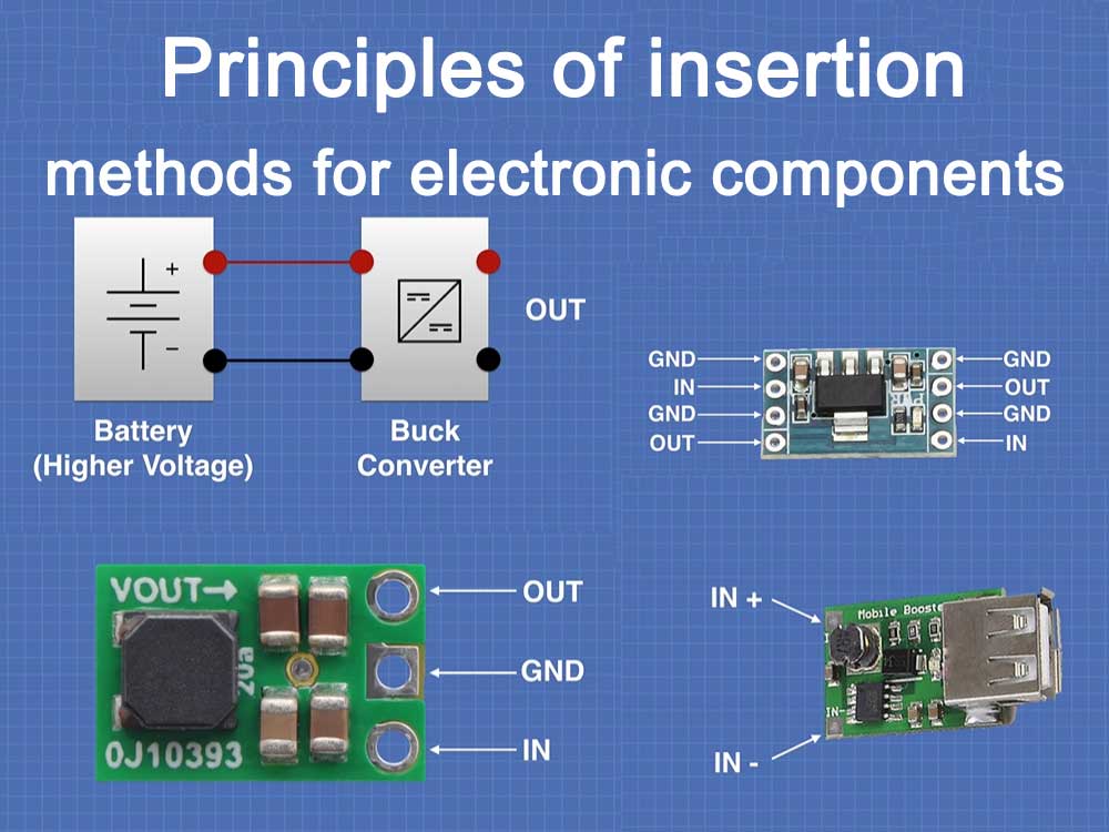
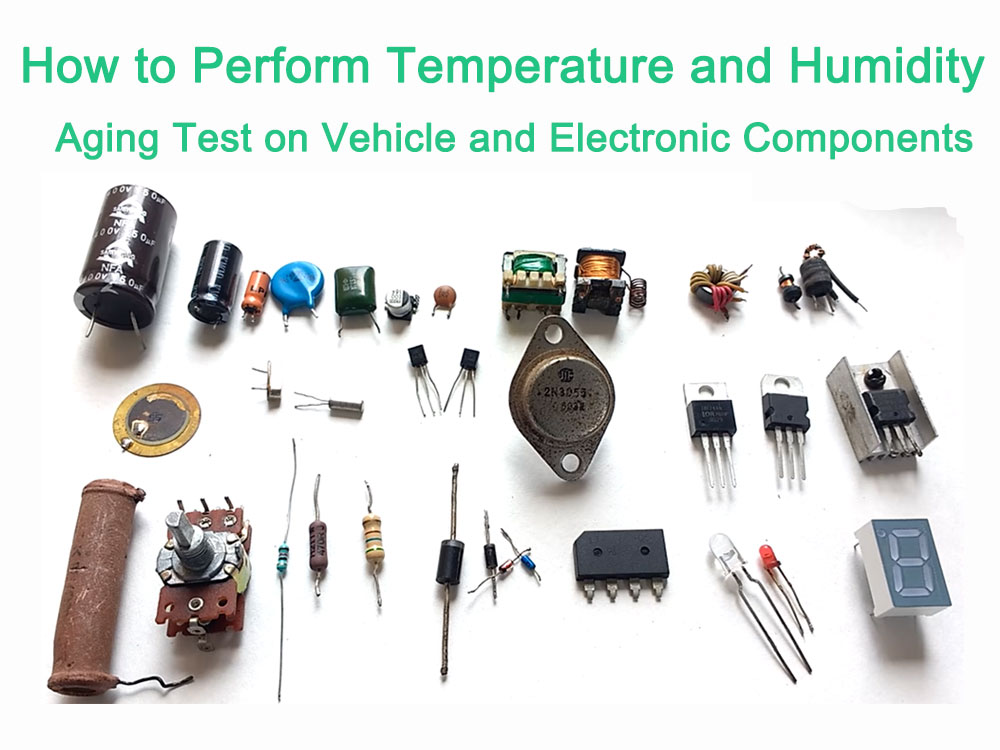
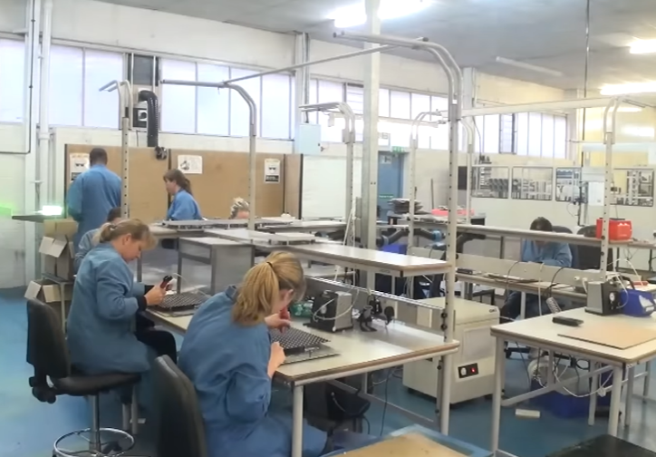
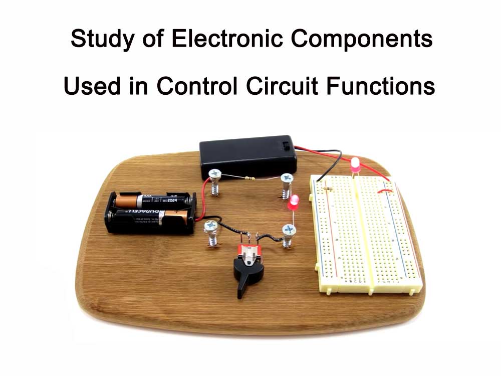
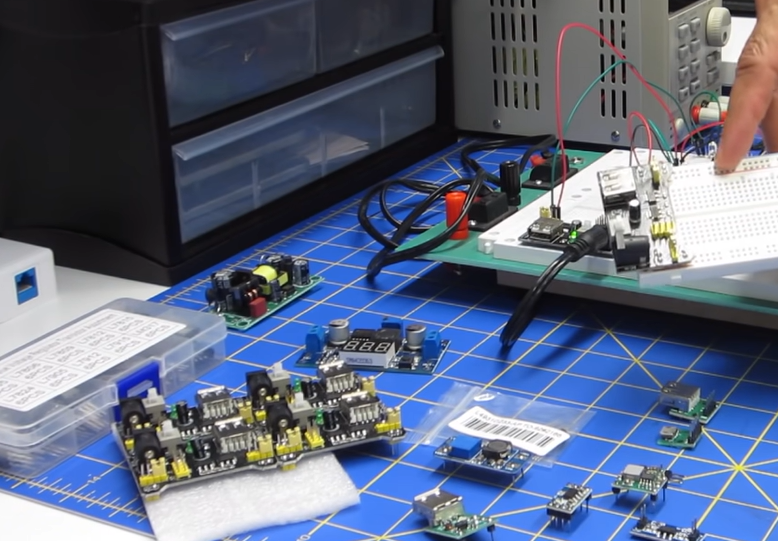
The following is a detailed introduction to the principles of electronic component insertion.
Principles of component insertion
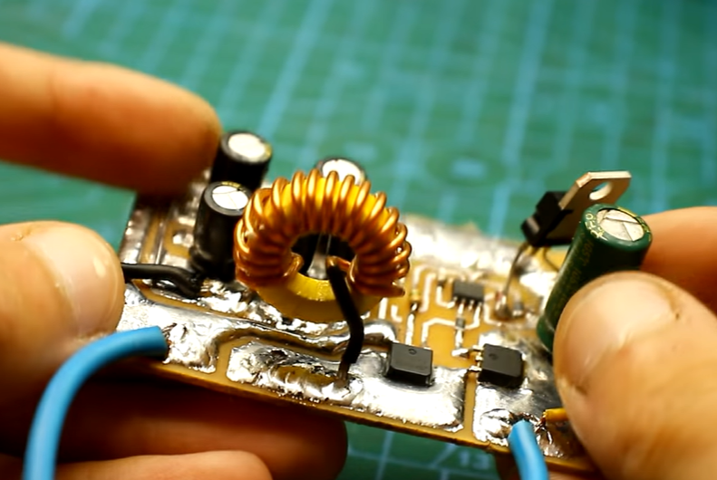
Polarity of components: When inserting components, the polarity of each component must be clear based on the circuit diagram and component specification table, and the correct direction must be ensured for installation.
Marking of components: All installed components must be clearly marked. These markings include component numbers, specifications, directions, etc. to facilitate subsequent debugging and maintenance.
Layout of components: The layout of components should be as uniform and symmetrical as possible in accordance with the requirements of circuit design to improve the overall aesthetics and reduce thermal stress caused by uneven heat distribution.
Fixing of components: Components should be fixed on the PCB board by welding, mechanical clamping, gluing, etc. During the fixing process, avoid applying excessive pressure or torque to the components to avoid damage.
Spacing of components: The spacing between components should be determined according to the requirements of the circuit and the production process. Proper spacing ensures the electrical performance of the circuit board and the operability of the production process.
Identification of components: Components should be clearly marked, including component numbers, specifications, directions, etc., to facilitate subsequent debugging and maintenance.
Choice of insertion method
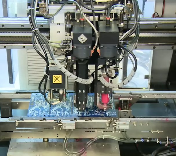
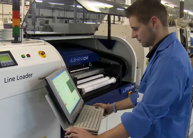
Manual insertion and automatic insertion: According to the requirements of production scale and automation level, you can choose manual insertion or automatic insertion. Manual insertion is more flexible and suitable for small batch production and maintenance; automatic insertion is more efficient and suitable for mass production.
Direct plug-in and surface mount: There are two methods of component insertion: direct plug-in and surface mount. In-line components can be directly inserted into the holes of the PCB board; surface mount components are directly attached to the surface of the PCB board. Surface mounting has the advantages of small size, light weight, and high reliability, but the manufacturing cost is high.
Ordinary plug-in and special plug-in: For some circuit boards with special requirements, such as high-density and high-reliability aerospace fields, special plug-in methods are required, such as vertical installation, flip-chip welding, etc.
Principles and key points of instrumentation
Ensure electrical performance: When inserting components, ensure that the electrical performance of the circuit board is met. For example, for some high-frequency signal lines, avoid excessively long traces or right-angle bends to reduce signal loss and noise.
Heat dissipation design: For some high-power components, heat dissipation issues need to be considered. Good heat dissipation can be ensured by properly arranging the radiator or increasing the spacing between components.
Prevent electromagnetic interference: When inserting components, electromagnetic interference issues should be considered. The impact of electromagnetic interference on circuit performance can be reduced by rationally arranging components and adding shielding measures.
Convenient maintenance and testing: When inserting components, subsequent maintenance and testing should be considered. Test points can be set up and clearly marked to facilitate maintenance personnel for inspection and repair.
Consider manufacturing costs: On the premise of meeting performance requirements, manufacturing costs should be reduced as much as possible. This can be achieved by optimizing circuit design, selecting appropriate components and insertion methods.
Practical application case analysis
In actual applications, it is necessary to choose the appropriate insertion method according to specific application scenarios and needs. For example, for some aerospace fields with high reliability requirements, special insertion methods can be used to ensure the performance and reliability of circuit boards; for some consumer electronics products, automated insertion methods can be used to improve production efficiency.
To sum up, the principle of insertion method of electronic components is an important part of the electronic assembly process. During the plug-in process, certain principles and key points need to be followed, and multiple factors such as electrical performance, reliability, and manufacturing cost must be comprehensively considered. The correct insertion method can ensure the performance and reliability of the circuit board, improve production efficiency, and reduce maintenance costs.
Frequently Asked Questions on the Principles of Inserting Electronic Components
Why do we need to clean electronic components before inserting them?
Before electronic components are inserted, the printed circuit board must be cleaned to remove impurities such as dirt, dust, and oxides on the surface. These impurities may cause short circuits, open circuits on the circuit board, or affect the stability of components.
Why can’t the pins of electronic components be bent?
The pins of electronic components cannot be bent, because bent pins may short-circuit or have poor contact with adjacent pins, causing circuit failure. In addition, lead bending can affect the mechanical properties and reliability of components.
How to avoid damage to electronic components during the insertion process?
When inserting electronic components, ensure that the insertion direction is correct and the force is moderate, and avoid using brute force. At the same time, the principles of first small then large, first low then high, first light then heavy should be followed to avoid damage to other installed components.
How to ensure the stability of electronic component insertion?
In order to ensure the stability of electronic component insertion, the insertion should be carried out according to a reasonable layout and arrangement to ensure that each component can be firmly fixed on the printed circuit board. At the same time, an appropriate amount of solder should be used and the welding quality should be ensured to prevent problems such as desoldering and virtual soldering.
How to identify the quality of electronic components?
Before insertion, the quality of electronic components should be checked. Detection can be done through visual inspection, measurement and testing. If necessary, use a magnifying glass or microscope for a more detailed inspection. If there are any damaged or unqualified components, they should be replaced in time.
Transistor is the most basic semiconductor device, its function is signal amplification and switching control.
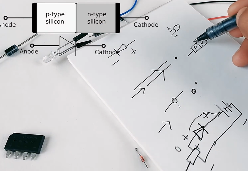
Diodes have unidirectional conductivity and are widely used in rectification and detection circuits. Integrated circuits integrate multiple electronic components on a substrate to achieve specific functions, greatly simplifying circuit design and assembly processes.
Here are the top 12 semiconductor device examples on YouTube:
Diode
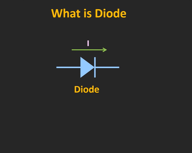
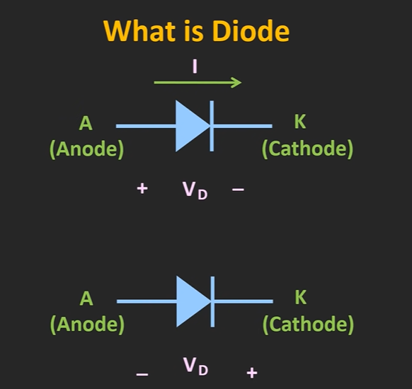
A diode is an electronic device made of semiconductor materials (silicon, selenium, germanium, etc.). It has two electrodes, one is positive and the other is negative.
When a forward voltage is applied between the two poles of the diode, the diode conducts; when a reverse voltage is applied, the diode turns off. Therefore, the diode has unidirectional conductivity.
When it is turned on, the direction of current flows from the anode through the tube to the cathode. Diodes are one of the earliest semiconductor devices and are used in a wide range of applications.
Triode
Triode is a semiconductor device that controls current. Its function is to amplify weak signals into electrical signals with larger amplitudes. It is also used as a contactless switch. In fact, a triode is composed of two diodes, so it has the characteristic of unidirectional conduction.
The transistor is made of two PN junctions that are very close to each other on a semiconductor substrate. The two PN junctions divide the entire semiconductor into three parts. The middle part is the base area, and the two sides are the emitter area and the collector area. The arrangement is PNP and NPN. When the transistor is in working condition, its base current Ib controls the collector current Ic, and the emitter current Ie is equal to the collector current Ic minus the base current Ib, that is, Ic=Ib+Ie.
The functions of the transistor include amplifying weak signals into electrical signals with larger amplitudes and serving as contactless switches. In electronic circuits, triodes are often used as amplifiers or switching circuits.
Darlington tube
A Darlington Transistor is a compound semiconductor device composed of two bipolar transistors whose output current is twice the input current. Darlington tubes have a very high amplification factor, which can reach hundreds or even thousands of times, so they are widely used in high-amplification circuits.
Darlington tubes are characterized by high current gain and low noise performance, and can achieve linear amplification of current. Due to its high amplification and low noise characteristics, Darlington tubes are widely used in audio amplifiers, servo systems, control systems and other fields. In addition, it can also be used in high-power switching circuits, motor drives, power amplification and other fields.
There are two basic types of Darlington tubes: coemitter-cobase and cobase-cobase. The cascode-cascode Darlington connects the collectors of two transistors. The input signal is input from the base of the first transistor, and the output signal is output from the collector of the second transistor. Common-base Darlington connects the bases of two transistors, the input signal is applied to the bases of both transistors at the same time, and the output signal is output from the collector of the first transistor.
In short, the Darlington tube is a high-performance, high-reliability semiconductor device with wide application prospects and market demand. As technology continues to advance and application demands continue to grow, the design and manufacturing technology of Darlington tubes will continue to develop and improve.
LED semiconductor devices
LED (Light Emitting Diode) is a solid-state semiconductor device that can directly convert electrical energy into light energy. Its core part is a semiconductor wafer. When current passes through this wafer, electrons and holes recombine and emit energy in the form of photons.
The LED chip is composed of two parts, one part is a P-type semiconductor, where holes dominate; the other end is an N-type semiconductor, where electrons are dominant. When these two semiconductors are connected, a P-N junction is formed between them.
When an electric current acts on this wafer through a wire, electrons are pushed to the P region, where they recombine with holes and then emit energy in the form of photons.
The main function of an LED is to emit light, and the color of its light can be adjusted by changing the semiconductor material. The color of an LED depends on the material forming the P-N junction, and the wavelength and color of the light are determined by the energy gap of the semiconductor.
For example, red LEDs have an energy gap of approximately 1.63eV, while blue and green LEDs have higher energy gaps of approximately 2.26eV and 2.58eV respectively.
LEDs are widely used in lighting, display, signal indication and other fields. For example, in displays, LEDs can be used as backlight sources or directly as display pixels; in traffic lights, LEDs can be used to make red, yellow, and green signal lights; in cars, LEDs can be used for headlights; in decorative lighting , LEDs can be used to create a variety of colorful and flashing effects.
Field Effect Transistor
Field Effect Transistor (FET) is a common semiconductor device. Its working principle is to control the conductive properties of semiconductor materials by changing the electric field, thereby achieving signal amplification or switching control.
A field effect transistor is mainly composed of three electrodes, namely source, gate and drain. When a voltage is applied between the gate and source, an electric field is created in the semiconductor material, controlling the current flow between the source and drain.
Since the conductive properties of field effect transistors are related to the intensity of the electric field, they have high input impedance and noise suppression capabilities, which makes field effect transistors widely used in many fields.
According to different structures and working principles, field effect transistors can be divided into junction field effect transistors (JFET) and metal oxide semiconductor field effect transistors (MOSFET). Among them, MOSFET is one of the most widely used field effect transistors at present.
It has the characteristics of high speed, low noise, low power consumption, etc., and is widely used in amplifiers, switching power supplies, motor drives and other fields.
In short, the field effect transistor is a high-performance, high-reliability semiconductor device with wide application prospects and market demand.
As technology continues to advance and application demands continue to grow, the design and manufacturing technology of field effect transistors will continue to develop and improve.
Thyristor
Thyristor is the abbreviation of thyristor, also known as silicon controlled rectifier. It was previously referred to as silicon controlled rectifier. It is a PNPN four-layer semiconductor structure with three poles: anode, cathode and gate.
The working conditions of the thyristor are: forward voltage is applied and the gate has trigger current. Its derivative devices include: fast thyristor, bidirectional thyristor, reverse conduction thyristor, light-controlled thyristor, etc. It is a high-power switching semiconductor device, represented by the text symbols “V” and “VT” in the circuit (represented by the letters “SCR” in the old standard).
Thyristors have the characteristics of silicon rectifier devices and can work under high voltage and large current conditions, and their working process can be controlled.
They are widely used in controlled rectification, AC voltage regulation, non-contact electronic switches, inverters and frequency conversion electronics. in the circuit.
An integrated circuit is a miniature electronic device or component that interconnects the transistors, resistors, capacitors, inductors and other components and wiring required in a circuit, and is made on a small or several small semiconductor wafers or dielectric substrates.
It is then packaged in a tube and becomes a microstructure with the required circuit functions. The inventors of the integrated circuit are Jack Kilby (integrated circuits based on germanium (Ge)) and Robert Noyce (integrated circuits based on silicon (Si)).
Integrated circuits play an important role in modern electronic equipment. It is the core part of electronic equipment and can realize various complex functions, such as computing, communication, control, etc. The manufacturing of integrated circuits requires multiple process steps, including oxidation, photolithography, diffusion, epitaxy, aluminum evaporation, etc.
The manufacturing process is extremely complex. With the development of technology, the integration level of integrated circuits continues to increase, the performance becomes more and more powerful, and the size is getting smaller and the power consumption is getting lower and lower.
Integrated circuits are widely used in almost every field, such as computers, communications, consumer electronics, medical care, industrial control, etc. For example, the CPU in a computer, the GPU in a graphics card, and the chip in a mobile phone are all examples of integrated circuits. In the future, with the advancement of technology and the expansion of applications, integrated circuits will continue to develop and grow.
Power Electronics
Power Electronic Devices, also known as power semiconductor devices, are mainly used for high-power electronic devices in power conversion and control circuits of power equipment (usually referring to currents ranging from tens to thousands of amperes and voltages of hundreds of volts above).
Power electronic devices can be divided into semi-controlled devices, fully controlled devices and uncontrollable devices.
Thyristors are semi-controlled devices with the highest voltage and current capacity among all devices; power diodes are uncontrollable devices with simple structure and principle and reliable operation; they can also be divided into voltage-driven devices and current-driven devices, among which GTO, GTR is a current-driven device, and IGBT and power MOSFET are voltage-driven devices.
Microelectromechanical Systems (MEMS) devices
A microelectromechanical system (MEMS) device is a microdevice or system that integrates micromechanisms, microsensors, microactuators, and signal processing and control circuits. It is based on micro/nano technology and uses semiconductor materials and processes for design and manufacturing. It has the advantages of small size, light weight, low power consumption and high reliability.
The manufacturing of MEMS devices requires multiple process steps, including material selection, structural design, manufacturing process, packaging, etc.
The manufacturing process requires the use of micro-machining technologies, such as photolithography, etching, thin film deposition, etc., to achieve micron-level precision processing. Common MEMS devices include micro-sensors, micro-actuators, micro-pumps, micro-valves, micro-gears, micro-springs and micro-optical devices.
MEMS devices are widely used in various fields, such as automotive electronics, medical equipment, aerospace, environmental monitoring, consumer electronics, etc.
For example, the acceleration sensor in a car airbag is a MEMS device, used to detect changes in acceleration during a collision; the gyroscope and accelerometer in a smartphone are also MEMS devices, used to implement functions such as automatic rotation and gesture recognition.
In the future, with the development of MEMS technology and the expansion of applications, MEMS devices will become more intelligent and multi-functional, and are expected to play a greater role in the Internet of Things, smart manufacturing and other fields.
Optical semiconductor devices (such as lasers, photodetectors, etc.)
Optical semiconductor devices refer to devices made by utilizing the optical properties of semiconductors and are mainly used in the field of optoelectronics. The following are some common optical semiconductor devices:
Light-emitting diode (LED)
An electroluminescent device that converts electrical energy into light radiation.
Laser diode (LD)
A semiconductor device that generates laser light, often used in fiber optic communications, optical disk storage and other fields.
Optical detector
A device that converts optical signals into electrical signals. It is often used in optical fiber communications, environmental monitoring and other fields.
Photomultiplier tube (PMT)
A highly sensitive light detector commonly used in night vision, spectral analysis and other fields.
Solar cell
A device that converts light energy into electrical energy and is the core part of the solar power generation system.
Photoconductivity sensor
A sensor made using the photoconductivity effect of semiconductors, which is often used in fields such as light intensity and light spot positioning.
Phototransistor
A semiconductor device that uses light signals to control current. It is often used in optical communications, light detection and other fields.
Optical crystal
A semiconductor material that can control the propagation of light waves. It is often used in fields such as generating lasers and modulating optical signals.
These optical semiconductor devices play an important role in the field of optoelectronics and promote the development and application of optoelectronic technology.
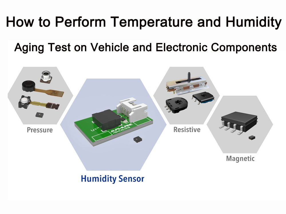
Sensors (such as temperature sensors, pressure sensors, etc.)
A sensor is a detection device that can sense measured information and convert the sensed information into electrical signals or other required forms of information output according to certain rules to meet the needs of information transmission, processing, storage, display, recording and control. Require. Semiconductor sensors refer to sensors that use the physical or chemical effects of semiconductors to sense and convert physical quantities, chemical quantities, or biological quantities.
There are many types of semiconductor sensors, including temperature sensors, humidity sensors, pressure sensors, flow sensors, gas sensors, ion sensors, etc.
They have the advantages of small size, high precision, good stability, and strong anti-interference ability, so they are widely used in industrial automation, environmental protection, medical care, smart home and other fields.
The working principle of semiconductor sensors is mainly based on the physical or chemical effects of semiconductors.
For example, semiconductor temperature sensors work based on the Seebeck effect or Peltier effect; semiconductor gas sensors use the adsorption of gas on the semiconductor surface to cause changes in the resistance or capacitance of the semiconductor to detect The composition and concentration of the gas.
With the development of the Internet of Things and smart devices, the application prospects of semiconductor sensors are even broader.
In the future, semiconductor sensors will be more intelligent, miniaturized, and multifunctional, bringing more convenience to human production and life.
Application Specific Integrated Circuit (ASIC)
Application-Specific Integrated Circuit (ASIC) is a customized, dedicated integrated circuit chip that is usually designed and manufactured according to the needs of specific users and the requirements of specific electronic systems.
ASIC chips have the advantages of high integration, high performance, low power consumption, and high reliability, so they are widely used in many fields.
ASIC chips go through multiple stages in their design and fabrication. First, the function and performance parameters of the chip need to be determined according to the user’s needs, and then logic design, circuit design, layout design, etc. are carried out. Then, the designed layout is handed over to the semiconductor manufacturing factory for processing, and finally the ASIC chip is obtained.
ASIC chips can be divided into two types: fully custom ASIC and semi-custom ASIC. A fully custom ASIC is a chip that is completely customized according to the user’s needs and requires the entire circuit to be designed and manufactured; while a semi-custom ASIC can be pieced together using cells from a standard cell library and only requires the design of part of the circuit.
ASIC chips are widely used in many fields, such as communications, military, aerospace, industrial control, consumer electronics, etc.
For example, in the field of communications, ASIC chips can be used for baseband processing, radio frequency processing, optical communications, etc.; in the military field, ASIC chips can be used for missile guidance, radar signal processing, etc.
In short, application specific integrated circuit (ASIC) is a high-performance, high-reliability semiconductor device with wide application prospects and market demand. As technology continues to advance and application requirements continue to grow, the design and manufacturing technology of ASIC chips will continue to develop and improve.
These semiconductor devices are widely used in various fields of electronic equipment and systems. For example, their application examples can be found in computers, communications, consumer electronics, industrial automation, automotive electronics and other fields.
Semiconductor purchasing wholesaler
Semiconductor device suppliersrefer to companies that provide semiconductor device products. These companies usually have cooperative relationships with semiconductor manufacturing plants, electronic manufacturers, etc., and provide various types of semiconductor devices, such as transistors, diodes, integrated circuits, etc. Supplier strength and credibility are critical to electronics manufacturers because the quality and reliability of their products directly affects the performance of the final product.
Top 12 Semiconductor Device Examples FAQs on YouTube
What is the difference between MOSFET and junction field effect transistor?
MOSFETs and junction field effect transistors are both semiconductor devices, but there are significant differences. MOSFET is a voltage-controlled device that controls the drain current by controlling the gate voltage. It has the advantages of strong driving capability, high reliability, small size, and low power consumption. It is suitable for electronic switches, signal amplification, rectifiers and other fields. The junction field effect transistor is a current-controlled device that controls the drain current by controlling the base current. It has the advantages of high voltage gain, low noise, and low distortion, and is suitable for low-frequency amplification applications. Therefore, MOSFET and junction field effect transistor have their own characteristics in structure and application, and they need to be selected according to specific needs.
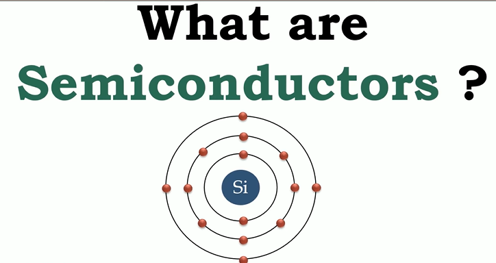
What is a semiconductor?
Semiconductors refer to materials whose electrical conductivity at room temperature is between conductors and insulators.
What are the advantages and disadvantages of MOSFET and junction field effect transistor?
MOSFETs and junction field effect transistors each have their own advantages and disadvantages. MOSFET has the advantages of high input impedance, low noise, low power consumption, and high switching speed, and is suitable for high-frequency applications, such as audio amplifiers and radio frequency receivers. The junction field effect transistor has the advantages of high reliability, stability, and strong controllability, and is suitable for switching, amplification, and adjustment functions in analog circuits and digital circuits.
What are the advantages and disadvantages of thyristor 7BA1?
The advantages of thyristor 7BA1 are high efficiency and high reliability, but the disadvantage is limited fast turn-on and turn-off capabilities.
What is thyristor 7BA1?
Thyristor 7BA1 is a unidirectional silicon controlled rectifier device, mainly used in AC voltage regulation, motor control, lighting control and other fields.
What is a thyristor switch?
Thyristor switch is a high-power switching semiconductor device with controllable unidirectional conductivity.
What is a PN channel field effect transistor?
A PN channel field effect transistor is a semiconductor device whose conductive channel is formed by a structure between a P-type semiconductor and an N-type semiconductor. By controlling the gate voltage, the carrier distribution in the channel can be modulated, thereby controlling the drain current. size. This device has the advantages of high input impedance, low noise, and low power consumption, and is widely used in electronic circuits.
What is the difference between integrated circuits and semiconductors?
An integrated circuit is a miniature electronic component that integrates multiple electronic components on a substrate to complete certain circuit or system functions. Semiconductors refer to materials whose electrical conductivity at room temperature is between conductors and insulators. Integrated circuits are made of semiconductor materials and implement various circuit functions in a tiny volume.
What are semi-controlled devices and uncontrollable devices of power electronic devices?
Power electronic devices can be divided into semi-controlled devices and uncontrollable devices according to their control characteristics. A semi-controlled device is a device that can be controlled to be turned on but cannot be controlled to turn off through a control signal, such as a thyristor. Uncontrollable devices are devices whose on-off is completely determined by the operating voltage or current, such as power diodes.
Which integrated circuit or semiconductor is more suitable for computer CPU chips?
Both integrated circuits and semiconductors can be used as computer CPU chips, but integrated circuits are more suitable for large-scale integration, while semiconductors are more suitable for small-scale integration. Therefore, integrated circuits are more common in the manufacture of computer CPU chips.
Which is more advanced, integrated circuits or semiconductors?
There is no obvious advanced difference between integrated circuits and semiconductors. Both are important components of modern electronic technology, and each has different applications and advantages in specific fields. Integrated circuits are microelectronic components that integrate multiple electronic components on a substrate to complete certain circuit or system functions. They have the advantages of miniaturization, high performance, and low cost. Semiconductors refer to materials whose electrical conductivity at room temperature is between conductors and insulators. They have a wide range of applications and are of important strategic significance. In some specific cases, integrated circuits and semiconductors may be used complementary or alternatively to each other, so one cannot simply say which one is more advanced.
What is a computer CPU chip?
The computer CPU chip is the physical implementation of the Central Processing Unit (Central Processing Unit) and is the core component of the computer responsible for executing instructions, processing data and controlling hardware.
What is a power diode?
Power diode is an electronic component that can withstand high voltage and large current. It is widely used in rectifier equipment of various high-voltage DC power supplies.
What is a thyristor power diode?
Thyristor power diode is a semiconductor device capable of controlling large current and voltage, and is widely used in power electronic equipment and strong current control systems. It is characterized by realizing unidirectional conduction within a larger current and voltage range and being able to control a larger load current by applying a smaller control signal.
What is a thyristor rectifier?
A thyristor rectifier is a power electronic device that uses thyristors to convert AC to DC power. It consists of multiple thyristors, each of which controls the behavior of the current. The thyristor rectifier accepts alternating current input, and after rectification and transformation, outputs stable direct current.
What are NPN and PNP transistors?
NPN type and PNP type transistors are two different types and structures of semiconductor transistors. The main difference lies in the voltage relationship between their base and emitter and the current flow direction.
What is a PN junction?
The PN junction is a semiconductor structure composed of an N-type semiconductor and a P-type semiconductor. The interface between the two semiconductors forms a special thin layer with unidirectional conductivity. In P-type semiconductors, holes are majority carriers, and in N-type semiconductors, electrons are majority carriers. When P-type and N-type semiconductors are combined, due to the difference in carrier concentration, some multipliers diffuse through the interface to the other side, leaving immovable charged ions, forming a space charge region. In the PN junction, the diffusion of electrons and holes causes current to flow from the N-type side to the P-type side, forming a forward current. At the same time, the reverse current is very small. This phenomenon is called the unidirectional conductivity of the PN junction.
What is a silicon controlled rectifier?
Silicon controlled rectifier is an electronic device that uses the characteristics of silicon controlled rectifier (SCR) to control and regulate current. SCRs have many advantages such as high efficiency, no mechanical noise and wear, fast response, small size, and light weight. They are widely used in industrial automation systems, frequency conversion speed regulation, photovoltaic power generation and other fields.
What is AC to DC?
AC to DC is the process of converting alternating current into direct current, usually through a rectifier. A rectifier is an electronic device that converts alternating current into direct current. It is widely used in various situations that require direct current power. Its working principle is to rectify the positive and negative half cycles of alternating current into waveforms of opposite polarity of direct current through the unidirectional conductivity of the rectifier diode, so that the output terminal obtains stable direct current.
What is an inverter?
An inverter is an electronic device that converts DC power into AC power. It is commonly used in various situations where batteries or DC power supply need to be converted into AC power.
What is an antielectron hole?
Antielectron holes are a concept corresponding to ordinary electrons and holes, which exist in certain materials, such as wide bandgap semiconductor materials such as gallium nitride. Under the influence of a strong electric field, the electrons in gallium nitride will gain enough energy to jump into the conduction band, leaving a vacancy, that is, a hole. This hole is negatively charged and is called an antielectron hole.
Why can transistors amplify electrical signals?
Transistors can amplify electrical signals because the voltage relationship between their base and emitter and the direction of current flow can control the size and direction of the collector current, thereby amplifying the signal.
What brands of triodes are there?
Excellent transistor brands include ROHM, ONsemi, ST, WeEn, VISHAY, DIODES, China Resources Microelectronics, etc.
What material is gallium nitride?
Gallium nitride is an inorganic substance with the chemical formula GaN. It is a compound of nitrogen and gallium. It is a direct bandgap semiconductor and has been commonly used in light-emitting diodes since 1990. This compound has a structure similar to wurtzite, has high hardness and a large bandgap. It can be used in high-power, high-speed optoelectronic devices. For example, gallium nitride can be used in violet laser diodes, which can produce light without the use of nonlinear semiconductor-pumped solid-state lasers. Violet (405nm) laser. In addition, gallium nitride is also one of the core materials of the third generation semiconductor. It has the advantages of high switching frequency, large band gap, and lower on-resistance. This material is usually used in LED (lighting, display), radio frequency communications and In the field of high-frequency power devices, mobile phone fast charging is one of the representative applications of gallium nitride in the field of high-frequency power devices. Compared with traditional fast charging, gallium nitride fast charging has greater power density, faster charging speed, smaller size and easy portability, which can meet consumers’ dual needs for fast charging and lightweight electronic products.
What are the disadvantages of mems devices?
The shortcomings of MEMS devices mainly include insufficient mechanical strength and stability, high manufacturing costs, reliability issues, insufficient integration, and immature production processes.
What are the advantages of mems devices?
The advantage of MEMS devices is that they can realize micro-nanoscale measurement and perception of complex mechanical motion and various physical quantities (such as force, heat, light, sound, etc.), and have the characteristics of miniaturization, high precision, high reliability, low energy consumption, and low cost. and other advantages, so it is widely used in automobiles, aerospace, biomedical and other fields.
What are the advantages of MEMS devices?
The advantages of MEMS devices are: small size, light weight, low power consumption, high reliability, high sensitivity, easy integration, etc.
What are the characteristics of MEMS devices?
The main characteristics of MEMS devices are miniaturization, high precision, high reliability, low energy consumption, low cost, etc. In addition, MEMS devices also have the advantages of high sensitivity, fast response, and mass production. These characteristics make MEME devices have broad application prospects in many fields.
What is the difference between MEMS devices and silicon-based chips?
The main difference between MEMS devices and silicon-based chips is the manufacturing process and use. Silicon-based chips integrate multiple electronic components on a silicon chip to realize circuit and system functions. They are mainly used in the manufacturing of integrated circuits, such as computer processors, memories, etc. MEMS devices integrate tiny mechanical structures with electronic circuits and are mainly used in the manufacture of sensors, actuators and other devices, such as accelerometers, gyroscopes, etc. There are major differences between the two in terms of manufacturing processes, materials, structures, etc.
What are the applications of laser technology?
Laser technology is widely used in various fields, such as industrial production, medical care, military, scientific research, etc. For example, lasers are used to manufacture various materials, perform metal cutting, marking, welding, etc.; in the medical field, lasers are used in surgeries, treatment of various diseases, etc.; in the military field, lasers are used in guided weapons, lidar, etc. etc.; In the field of scientific research, lasers are used for spectral analysis, measurement, etc.
What is a laser transmitter?
A laser transmitter is a device that uses the principle of stimulated emission of light to generate and amplify laser light. It is an electronic light source device that can produce collimated, monochromatic and coherent beams. It usually consists of main components such as laser medium and pump source, and is widely used in various fields.
What is fiber optic transmission?
Fiber optic transmission is a communication method that uses optical fibers as transmission media, and information is transmitted through the transmission of optical signals in optical fibers. Optical fiber transmission has the advantages of long transmission distance, fast speed, wide frequency bandwidth, large information capacity, strong anti-interference ability, and good confidentiality. It is one of the main transmission methods of modern communication networks.
What are the characteristics of LED?
LED has the characteristics of high efficiency, environmental protection, safety, small size, fast response speed, impact resistance, good weather resistance, good directionality, rich colors, and long life.
The development history of optical semiconductor devices?
The development history of optical semiconductor devices can be traced back to the last century. With the continuous development of information technology, optical semiconductor devices have been widely used in communications, sensing, lighting and other fields. Among them, the invention and promotion of optical fibers made optical signal transmission possible, thus promoting the development of optical communication technology. In addition, the invention of lasers also provided important support for the development of optical semiconductor devices. Today, optical semiconductor devices have become an important part of modern information technology, bringing great convenience to people’s lives and work.
What are the advantages and disadvantages of optoelectronic semiconductor devices?
The advantages of optoelectronic semiconductor devices include high photoelectric conversion efficiency, high response speed, easy integration, etc. Its disadvantages include poor temperature stability and high noise.
What is a humidity sensor?
A humidity sensor is a sensor that senses humidity and converts it into a usable output signal. It is used to measure the humidity in the environment and provide associated electrical signals for further processing or control.
What types of sensor semiconductor devices are there?
There are mainly the following types of semiconductor devices for sensors: Resistive sensor: Uses the resistance change of semiconductor materials to measure parameters such as temperature, pressure, humidity, etc. Capacitive sensor: uses the capacitance change of semiconductor materials to measure parameters such as displacement, angle, vibration, etc. Voltage sensor: uses the voltage effect of semiconductor materials to measure parameters such as temperature, pressure, magnetic field, etc. Current sensor: Use the current effect of semiconductor materials to measure parameters such as temperature, pressure, humidity, etc. Hall sensor: uses the Hall effect of semiconductor materials to measure parameters such as magnetic field and current. These sensors are widely used in various fields, such as industrial automation control, environmental monitoring, medical equipment, aerospace and other fields.
What is a general-purpose integrated circuit?
A general-purpose integrated circuit refers to an integrated circuit that can realize a variety of different functions of electronic components integrated onto a chip. This kind of integrated circuit can realize various functions such as data processing and power control through electrostatic control, so it is widely used in various industries.
What does poor temperature stability mean?
Poor temperature stability means that during the working process of electronic components such as optoelectronic semiconductor devices, their performance parameters are easily affected by changes in ambient temperature, causing the output to be unstable or deviate from expected values.
What are co-emission-co-base Darlington tubes and co-base-co-base Darlington tubes?
Common-emitter-common-base Darlington tubes and common-base-complex Darlington tubes are two different types of Darlington tubes. The cascode-cascode Darlington is composed of two triodes, one of which acts as a basic amplifier and the other acts as an emitter follower. The two triodes are connected together through a common base. The common-base Darlington tube is composed of two triodes connected by a common base. Each triode has an independent base and collector, and they are connected together through a common emitter.
Which is better, Darlington or thyristor?
Darlington tubes and thyristors each have their own advantages and applicable scenarios, and they cannot be compared simply. Darlington is a high-amplification transistor that is often used in circuits that require large current drive, such as audio amplifiers, motor drives, etc. The thyristor is a silicon-controlled rectifier, mainly used for the control and regulation of alternating current, such as dimmers, power supplies, etc. Therefore, the choice of Darlington or thyristor should be decided based on actual needs and circuit requirements.
What is the essential difference between co-base and co-base?
The essential difference between common-base and common-base is the frequency of the input signal. The input signal to a cascode circuit is at a lower frequency, while the input signal to a cascode-to-cascode circuit is at a higher frequency.
What is a metal oxide semiconductor field effect transistor?
Metal oxide semiconductor field effect transistor is a field effect transistor that can be widely used in analog circuits and digital circuits, referred to as metal oxide half field effect transistor.
What are MOSFETs and junction field effect transistors?
MOSFET is the abbreviation of MetalOxideSemiconductorFieldEffectTransistor, which is translated into Chinese as “metal oxide semiconductor field effect transistor”. It is a device made of three materials: metal, oxide (SiO2 or SiN) and semiconductor. The junction field effect transistor is a three-terminal active device with amplification function. It is the simplest type of unipolar field effect transistor. It can be divided into N channel or P channel.
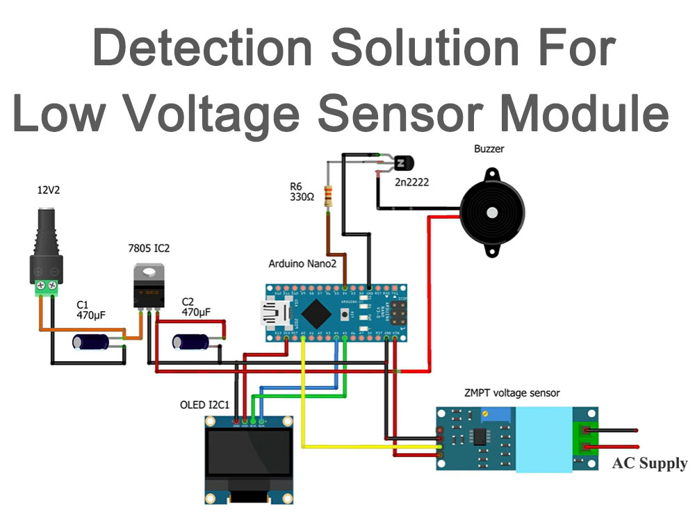
The low-voltage sensor module testing solution is a set of systematic and standardized testing processes, aiming to ensure that the module performance meets standards and has high reliability.
Through multiple tests such as environmental adaptability testing and electrical performance testing, the various indicators of the module are comprehensively evaluated to provide Provide a strong basis for product optimization.
Introduction
With the continuous development of industrial automation and intelligence, low-voltage sensor modules have been widely used in various equipment and systems.
In order to ensure the performance and quality of low-voltage sensor modules, it is crucial to develop an effective detection program.
This solution aims to conduct a comprehensive and accurate detection of the low-voltage sensor module to ensure its normal and stable operation.
Verify whether the performance indicators of the low-voltage sensor module meet the design requirements;
Test the performance of the low-voltage sensor module under actual working conditions;
Discover potential problems and failures of low-voltage sensor modules and reduce product repair rates;
Provide a basis for quality assessment and continuous improvement of low-voltage sensor modules.
Detection content and methods
Appearance inspection
Observe the appearance of the low-voltage sensor module and check whether there is damage, deformation, stains, etc., and whether the markings are clear and accurate.
Dimensional measurement
Use measuring tools to measure the critical dimensions of the low-voltage sensor module to ensure that it meets the design requirements.
Electrical performance test
Input voltage range test
Test whether the low-voltage sensor module can work normally within the specified input voltage range;
Output accuracy test
Pass the standard signal source input signal, measure the output signal of the low-voltage sensor module, and calculate its accuracy;
Response time test
When the input signal changes, measure the time it takes for the output signal of the low-voltage sensor module to change.
Environmental adaptability test
Temperature test
Test the performance of the low-voltage sensor module under different temperature conditions (such as -20°C, 25°C, 65°C, etc.);
Humidity test
Test the performance of the low-voltage sensor module under different humidity conditions;
Vibration test
Conduct a vibration test on the low-voltage sensor module to detect its anti-vibration performance.
Functional test
According to the specific functions of the low-voltage sensor module, simulate the actual working scenario and test its various functions.
Reliability test
Test the reliability of the low-voltage sensor module through accelerated life tests, fatigue tests and other methods.
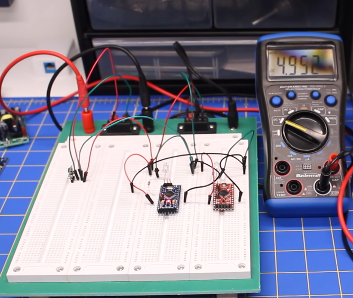
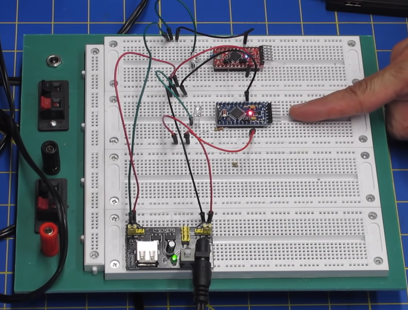
ZMPT101B 250V AC Voltage Sensor with Arduino, Voltage Monitoring
Prepare testing equipment and environment to ensure compliance with testing requirements;
Carry out appearance inspection and dimensional measurement, and record the inspection results;
Conduct electrical performance tests and record various parameter indicators;
Conduct environmental adaptability testing and record performance;
Conduct functional tests to verify the normality of various functions;
Conduct reliability testing to evaluate product life and reliability;
Analyze and evaluate the test results and form a test report;
According to the test report, unqualified products are processed, and qualified products are marked and stored in the warehouse.
Test report and summary
After completing the inspection of the low-voltage sensor module, a detailed inspection report should be prepared. The report should include the following:
Testing purposes and requirements;
Test content and methods;
Detection process and steps;
Test results and analysis;
Conclusion and recommendations.
Through the implementation of this solution, the low-voltage sensor module can be comprehensively and accurately tested to ensure that its performance and quality meet the requirements.
At the same time, this solution can also provide basis and suggestions for the continuous improvement and optimization of low-voltage sensor modules.
In practical applications, the solution can be adjusted and optimized according to specific circumstances to better meet actual needs.
What are the commonly used testing equipment for low-voltage sensor modules?
Commonly used testing equipment for low-voltage sensor modules include the following:
Signal source: used to provide standard signals to test the output accuracy and response time of the low-voltage sensor module.
Oscilloscope: used to measure and observe the output signal of the low-voltage sensor module to evaluate its performance.
Power supply: Provide stable DC or AC power to test the performance of the low-voltage sensor module under different input voltages.
Environmental chamber: used to simulate different temperature and humidity environments for environmental adaptability testing.
Vibration table: used to simulate a vibration environment to test the anti-vibration performance of the low-voltage sensor module.
Data acquisition and analysis system: used to collect and analyze test data of low-voltage sensor modules in order to quantitatively evaluate their performance.
Calibration equipment: used to calibrate testing equipment and tools to ensure the accuracy and reliability of testing results.
These devices are commonly used tools in low voltage sensor module testing, and which device is used depends on the testing needs and requirements.
When selecting testing equipment and tools, ensure that their accuracy, reliability and applicability meet the testing requirements.
What testing tools need to be included in the testing solution for low-voltage sensor modules?
The detection solution for the low-voltage sensor module needs to include the following detection tools:
Voltage test tool: such as a multimeter, used to measure whether the output voltage of the low-voltage sensor module is within the normal range.
Current testing tools: such as ammeters, used to test whether the output current is normal and whether it meets the relevant parameters of the sensor.
Internal resistance test tool: such as a multimeter or independent resistance meter, used to test whether the output resistance of the low-voltage sensor module is correct and stable.
Environmental adaptability testing equipment: such as temperature chambers, humidity chambers and shaking tables, etc., used to simulate different environmental conditions and test the performance of low-voltage sensor modules.
Signal source and oscilloscope: used to provide standard signals and measure the output signal of the low-voltage sensor module to evaluate its accuracy and response time.
Calibration equipment: used to calibrate testing equipment and tools to ensure the accuracy and reliability of testing results.
These tools are commonly used equipment in low-voltage sensor module testing. According to the specific testing needs and requirements, the corresponding equipment and tools can be selected for testing.
When selecting testing tools, ensure that their accuracy, reliability and applicability meet the testing requirements.
The low-pressure sensor module is an electronic component used to measure low-voltage, weak electrical signals. It can sense pressure changes of liquids, gases, solids and other substances and convert them into electrical signal output.
Why test the low voltage sensor module?
Low-voltage sensor modules are widely used in industrial automation and intelligence. It is crucial to detect their performance and quality to ensure their normal and stable operation, reduce product repair rates, and provide a basis for continuous improvement.
How to conduct electrical performance testing of low voltage sensor modules?
Electrical performance testing includes input voltage range testing, output accuracy testing, response time testing, etc. Input the signal through the standard signal source, measure the output signal of the low-voltage sensor module, calculate its accuracy, and observe the response time.
What does the low-voltage sensor module detect?
The testing content of low-voltage sensor modules mainly includes appearance inspection, dimensional measurement, electrical performance testing, environmental adaptability testing and functional testing, etc.
What does environmental suitability testing mean for low-voltage sensor modules?
The environmental adaptability test includes temperature test, humidity test and vibration test, etc. It is designed to detect the performance of the low-voltage sensor module under different environmental conditions to ensure that it can work normally in various environments.
How to evaluate the reliability of low voltage sensor modules?
Test the performance of the low-voltage sensor module under different stress conditions and evaluate its reliability through accelerated life tests, fatigue tests and other methods.
What issues should be paid attention to when testing low-voltage sensor modules?
During the testing process, you need to pay attention to preventing overloading, preventing static electricity, ensuring good grounding, etc. to ensure the accuracy and reliability of the testing results. At the same time, relevant safety regulations and operating procedures should be followed to ensure the safety of personnel and equipment.
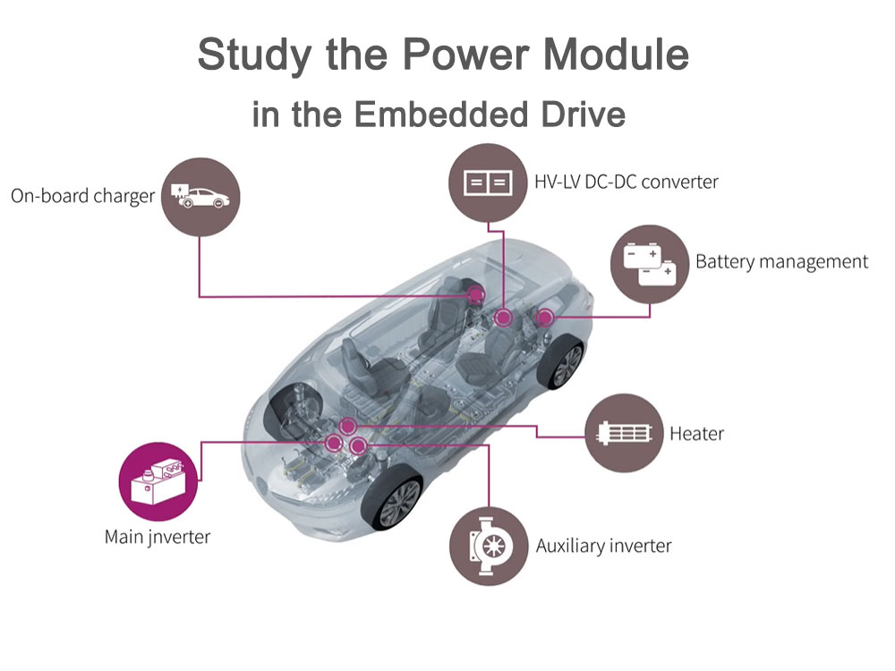
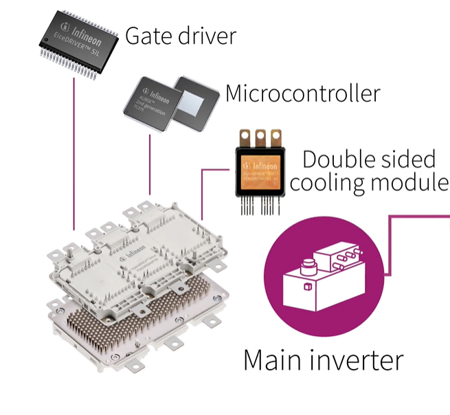
Research on power modules in embedded drives focuses on improving their energy efficiency, stability and lifespan to adapt to changing application requirements and promote energy conservation, emission reduction and system performance optimization.
Embedded discussion
With the rapid development of technology, the application of embedded systems in various fields is becoming more and more widely used, such as smart homes, industrial control, medical equipment, etc.
As an important part of the embedded system, the power module provides a stable energy source for the entire system, and its performance directly affects the stability and reliability of the entire system.
Therefore, in -depth research on the power module in embedded drivers has important theoretical and practical significance.
Overview of the power module in the embedded drive
The power module is the core part of the embedded drive, which is mainly responsible for converting the input power energy to the voltage and current suitable for embedded systems. It usually includes a rectifier circuit, filter circuit, voltage voltage circuit and other parts, which can realize functions such as voltage conversion, stability and protection.
The performance indicators of the power module mainly include efficiency, power density, and reliability. Among them, the efficiency determines the energy conversion efficiency of the power module, and is an important indicator of the performance of the power module. The power density reflects the performance of the volume and weight of the power module; reliability is an important thing for the power module to run stable for a long time. Assure.
The design of the power module requires comprehensive consideration of system requirements, electrical characteristics, and heat design. During the design process, the input and output voltage, current and other parameters of the power module need to be determined according to the maximum power consumption and voltage requirements of the system. At the same time, it is also necessary to consider the requirements of the efficiency, power density, and reliability of the power module to ensure that the power module can meet the long -term stable operation of the system.
In addition, in order to improve the reliability of the power module, a series of optimization measures are needed, such as choosing high-quality electronic components, optimizing circuit design, and strengthening heat dissipation design.
How does the power module in the embedded driver be designed with the power module
In the cooling design of the power module in the embedded drive, the main consider how to effectively export the heat from the power module and reduce its working temperature to ensure the stable operation of the power module and extend its service life. Here are some points of some cooling design:
Understand the heat source: First of all, you need to understand the main thermal sources in the power module, such as power semiconductors, inductors and capacitors. These components generate a lot of calories when converting electrical energy.
Natural cooling or forced cooling: According to the heat dissipation needs of the power module, you can choose natural cooling or forced cooling method. Natural cooling mainly relies on the natural flow of air to dissipate heat, which is suitable for lower thermal density. For compulsory cooling, it is necessary to use a fan or other forced ventilation equipment to be suitable for high -heat flow density.
The radiator design: If you need to use a radiator, you should choose the appropriate material (such as copper or aluminum) and shape to effectively export the heat from the power module. At the same time, the surface area of the radiator should be large enough to quickly emit calories.
Heating material: The heat conduction material (such as thermal grease or thermal pad) should be used between the power module and the radiator to transmit the heat from the power module to the radiator.
Isolation and protection: In order to prevent dust and other impurities from affecting the heat dissipation effect, appropriate protection and isolation measures should be set around the power module.
Monitoring and control: You can install the temperature sensor to monitor the working temperature of the power module, and use the control circuit to adjust the working state of the power module to maintain it within the appropriate temperature range.
Consider cost and space limit: In the design of heat dissipation, cost and space restrictions should be considered. Select the appropriate heat dissipation solution to meet the heat dissipation needs of the power module, and also consider the cost and size requirements of the product.
In short, in the cooling design of the power module in the embedded drive, multiple factors need to be comprehensively considered, such as heat sources, heat dissipation methods, heat sink design, heat conduction materials, protection measures, cost and space restrictions. Through a reasonable heat dissipation design, the working temperature of the power module can be effectively reduced to ensure its stable operation and extend its service life.
What is the difference between linear power module and switching power module
There are significant differences in linear power modules and switching power modules in multiple aspects:
Working principle: The working principle of the linear power module is to reduce the voltage and stable output through the coil transformer. The working principle of the switching power module uses the switch device (such as MOSFET) to convey and adjust the voltage by high frequency switching.
Efficiency: The efficiency of the switching power module is usually high, which can reach more than 80%of the energy conversion efficiency, and the efficiency of linear power modules is relatively low, generally between 50%and 60%.
Volume and weight: Because the switching power module uses a high -frequency switch to switch to achieve voltage conversion, its components can complete the voltage conversion in a smaller space, so the volume is small and the weight is relatively light. The linear power module needs to use large coil transformers and radiator components, and the volume and weight are relatively large.
Cost: Generally, the manufacturing cost of switching power modules is relatively low because they use less materials and components. The manufacturing cost of linear power modules is relatively high because more coil transformers and larger radiators need to be used.
Stability: Linear power modules usually have lower noise and good stability, and can provide clean output power. The switching power module may produce some electromagnetic interference and noise due to high -frequency switching.
In summary, linear power modules and switching power modules have their own advantages and disadvantages in terms of efficiency, volume, weight, cost, and stability. In practical applications, you can choose the appropriate power module type according to the needs.
Are there any environmentally friendly power modules, can I introduce it?
Environmental protection power module refers to the power module that meets environmental protection requirements. It uses environmental protection materials and production processes, which has a small impact on the environment.
Here are some common environmental protection power modules:
Green power module: The green power module is an efficient power -saving power module. It uses advanced control technology and high -efficiency switching power supply. It has the characteristics of energy saving, low noise, and low pollution. It is in line with the development trend of computer technology and can be recycled and reuse after the service life is over.
Switching power module: The switching power module is a small, high-efficiency, and high reliability power module. It uses switch tube or power MOSFET and other devices to achieve voltage conversion and adjustment through high -frequency switch switching. It has the advantages of small size, light weight, high efficiency, high reliability, and meets the requirements of energy saving and emission reduction.
Converter: The converter can convert a fixed DC voltage to a variable DC voltage, which is applied to the field -free transmission and control of trackless trams, subway trains, electric vehicles. This power module uses advanced control technology to reduce energy consumption and improve energy utilization efficiency, and at the same time can reduce noise and pollution to the environment.
UPS: UPS (uninterrupted power supply) is a power module that can provide continuous stable power supply, which is mainly used in the fields of computer, communication systems and data storage devices. It can ensure the normal operation of the device and the integrity of data in the case of power outage or voltage fluctuations. The UPS power module adopts high -efficiency switching power supply technology and advanced uninterrupted power supply technology, which can reduce energy waste and environmental pollution.
These environmentally friendly power modules use environmentally friendly materials and advanced production processes, which have the characteristics of efficient, energy saving, low noise, low pollution, etc., and meet the current society’s requirements for environmental protection and sustainable development.
The latest development of the power module in the embedded drive
With the continuous advancement of technology, the power module in embedded drivers is also developing. At present, the switching power supply technology has become the mainstream, and it has the advantages of high efficiency, small volume, and light weight. At the same time, some new power management technologies have also emerged, such as distributed power management systems based on power electronic technology, high -density integration power modules based on magnetic components. The development of these new technologies provides more choices and possibilities for power modules in embedded drives.
In addition, in order to meet the needs of green and environmental protection, lead and halogen -free environmental protection power modules have also been widely used. These power modules have higher reliability and longer service life, which meets the current society’s requirements for environmental protection and sustainable development.
The power module in the embedded driver concludes
The power module in the embedded drive is an important guarantee for the stable operation of the entire system. With the continuous development of technology, the performance of the power module is also continuously improved, and the application of new power management technology and environmental protection power modules is becoming wider and wider.
In order to better meet the needs of the system, future power module design needs to pay more attention to the performance of efficiency, power density and reliability.
At the same time, with the development of emerging technologies such as artificial intelligence and the Internet of Things, the power module in the embedded drive also faces new challenges and opportunities. Therefore, we need to continuously study and explore to promote the continuous development and progress of power module technology in embedded drivers.
Frequently Ask Q & A in the power module in embedded drivers
What is the power module in an embedded drive?
The power module in the embedded driver is an energy converter in the entire system. It is responsible for converting the input electrical energy into voltage and current suitable for embedded systems to provide stable power supply for each part of the system.
What are the main types of power modules?
There are two types of power modules: linear power modules and switching power modules. The linear power module adopts linear voltage voltage technology, which has a lower voltage noise and better stability. The switching power module uses switching voltage technology, which has high efficiency and miniaturization characteristics.
How to evaluate the performance of the power module?
The performance of the evaluation of the power module mainly includes indicators such as efficiency, power density, and reliability. Among them, efficiency determines the energy conversion efficiency of the power module, and the power density reflects the performance of the volume and weight of the power module, and reliability is an important guarantee for the power module to run stable for a long time.
How to choose the right power module?
Selecting the right power module needs to be determined according to the needs of the system and electrical characteristics. The factors that need to be considered include input output voltage, current, power density, efficiency, reliability, etc. In addition, the size, weight, and cost of the power module must be considered.
How to optimize the design of the power module?
Optimizing the design of the power module requires comprehensive consideration of multiple aspects. Including choosing high -quality electronic components, optimizing circuit design, strengthening heat dissipation design, etc. In addition, new power management technology and environmentally friendly power modules can be used to improve the performance and reliability of the power module.
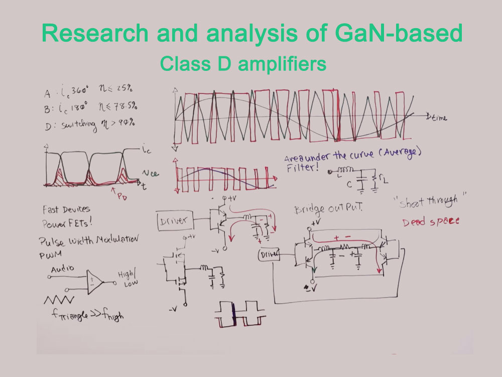
Research analysis of GaN-based Class D amplifiers: An in-depth discussion of the application of GaN materials in Class D amplifiers, and a comprehensive evaluation of its performance advantages, circuit design, stability and reliability.
It aims to promote the practical application of GaN technology in the field of high-efficiency power amplification and provide theoretical support for the development of green energy utilization and high-efficiency wireless communication systems.
Introduction
With the rapid development of communication technology, amplifiers are increasingly used in various wireless communication systems.
GaN (Gallium Nitride) material is widely used in the design of power amplifiers in the microwave and millimeter wave bands due to its superior electronic properties, including high breakdown electric field, high saturation electron velocity and high temperature stability.
As a high-efficiency amplifier, Class D amplifiers have significant advantages in reducing energy consumption and improving equipment stability. Therefore, the research on GaN-based Class D amplifiers has important practical significance.
GaN material characteristics and advantages
GaN material has the characteristics of wide bandgap, high saturation electron velocity and high breakdown electric field. These characteristics allow GaN-based devices to work in extreme environments such as high temperature, high pressure and high frequency.
In addition, GaN material also has excellent chemical stability and can resist various acid and alkali corrosion, greatly improving the reliability and stability of the device.
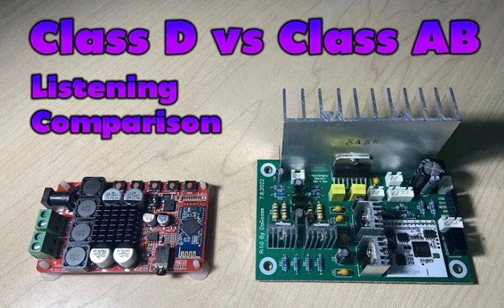
Working principle and advantages of Class D amplifier
Class D amplifier is a switch-mode amplifier. Its working principle is to convert the input signal into a pulse-width modulated square wave signal through a comparator and power switch, and then restore it to the original signal through a low-pass filter. Compared with traditional Class AB amplifiers, Class D amplifiers have higher efficiency because their power switches consume very little energy in the on and off states. In addition, the modulation method of the Class D amplifier results in low distortion of the output signal.
GaN-based Class D amplifier design
The main factors that need to be considered in the design of GaN-based Class D amplifiers are: the design of the input and output matching circuit, the design of the power switch, the design of the comparator circuit, and the design of the low-pass filter.
In these designs, the design of the power switch is key because the high electron mobility characteristics of GaN material enable it to support high-speed switching actions.
In addition, due to the low thermal conductivity of GaN materials, special consideration needs to be given to thermal management issues in the design to ensure that the amplifier can operate at normal temperatures.
GaN-based Class D Amplifier Research Results and Analysis
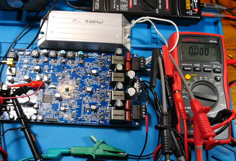
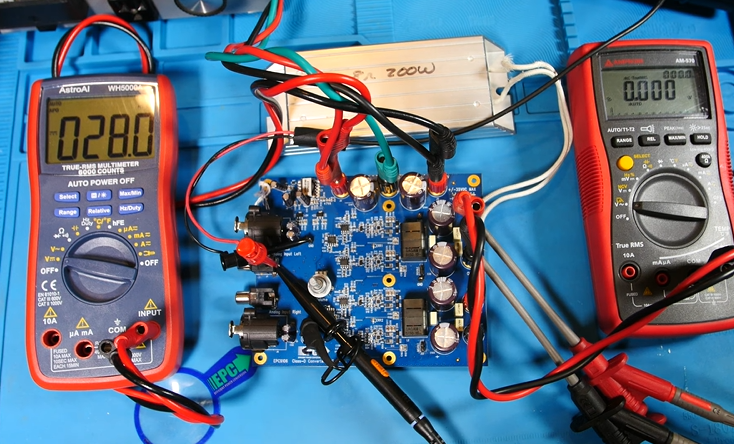
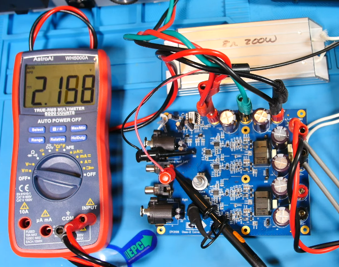
Class D Amplifier Bode Plot GaN systems vs EPC (Efficient Power Conversion) The GaN people – This video is about Class D Amplifier Bode Plot GaN systems vs EFC. I’ll test both the EPC GaN Class D Amplifier and the GaN Systems GaN Class D Amplifier. I’ll show the Bode plots of both amplifiers.
Through experimental tests, GaN-based Class D amplifiers have shown excellent performance in terms of efficiency, linearity, reliability, etc. In the high frequency band, its efficiency is as high as 85%, nearly double that of traditional silicon-based power amplifiers. In addition, the performance of GaN-based Class D amplifiers also shows good stability in high and low temperature environments.
Research conclusions and prospects of GaN-based Class D amplifiers
GaN-based Class D amplifiers provide new possibilities for next-generation wireless communication systems with their high efficiency, high linearity and excellent reliability. With the advancement of technology and in-depth research, the performance of GaN-based Class D amplifiers will be further improved, and its application prospects in communications, radar, electronic warfare and other fields will be broader.
Summary of GaN-based Class D Amplifiers
Through in-depth research on GaN-based Class D amplifiers, we not only have a deeper understanding of GaN materials and Class D amplifiers, but also provide strong theoretical support and practical guidance for practical applications.
Although GaN-based Class D amplifiers still face some challenges in practical applications, such as thermal management, capacitive load effects, etc., with the continuous emergence of new materials, new processes and new methods, we have reason to believe that these issues will be solved Effective solution.
In the future, GaN-based Class D amplifiers will play a more important role in improving communication system efficiency, reducing energy consumption, and improving equipment stability.
GaN stands for Gallium Nitride, that is, gallium nitride. It is a wide bandgap semiconductor material that is widely used in the design of power amplifiers in the microwave and millimeter wave bands because of its excellent electronic properties and high temperature stability.
What are the advantages of GaN?
The advantages of GaN are its high breakdown electric field, high saturation electron velocity, and high temperature stability. These characteristics allow GaN-based devices to operate in extreme environments such as high temperature, high pressure, and high frequency while maintaining excellent performance.
What is a Class D amplifier?
Class D amplifier is a switch-mode amplifier that converts the input signal into a pulse-width modulated square wave signal through a comparator and a power switch, and then restores it to the original signal through a low-pass filter. Compared with traditional Class AB amplifiers, Class D amplifiers have higher efficiency.
What are the difficulties in designing GaN-based Class D amplifiers?
The design difficulties of GaN-based Class D amplifiers mainly include the design of the input and output matching circuit, the design of the power switch, the design of the comparator circuit and the design of the low-pass filter. Among them, the design of the power switch is key because the high electron mobility characteristics of GaN materials require high-speed switching actions. Additionally, special considerations need to be made about thermal management.
What are the advantages of GaN-based Class D amplifiers?
The advantages of GaN-based Class D amplifiers mainly include high efficiency (such as high-frequency band efficiency up to 85%), high linearity and excellent reliability. These advantages make it an ideal choice for next-generation wireless communication systems.
What challenges do GaN-based Class D amplifiers face in their applications?
Challenges faced by GaN-based Class D amplifiers in applications include thermal management, capacitive load effects and other issues. These challenges require further research and resolution to achieve more stable and efficient applications.
How to evaluate the future development prospects of GaN-based Class D amplifiers?
GaN-based Class D amplifiers have broad prospects for future development. As new materials, new processes and new methods continue to emerge, its performance will be further improved. In fields such as communications, radar, and electronic warfare, GaN-based Class D amplifiers will play a more important role, providing strong support for improving communication system efficiency, reducing energy consumption, and improving equipment stability.
Therefore, research on the manufacturability of electronic components has become increasingly important. This article will provide a detailed introduction to the research on manufacturability of electronic components, including its research significance, main content, methods and technologies.
Manufacturability of electronic components refers to the feasibility, stability and reliability of components during the production process. It involves every aspect from design, material selection to process flow, ensuring that products can be put into production efficiently and at low cost.
In-depth research on the manufacturability of electronic components can help improve production efficiency, optimize product design, and reduce production costs.
Why does electronic component manufacturability exist
The significance of the manufacturability of electronic components is mainly reflected in the following aspects:
Solve manufacturing problems
The manufacturing process of electronic components involves many complex issues, such as process control, material selection, equipment accuracy, etc. Manufacturability research is to solve these manufacturing problems and ensure that components can be produced efficiently, stably and reliably.
Improve production efficiency
By optimizing the manufacturing process, reducing production links, and improving the accuracy and reliability of production equipment, the production efficiency of electronic components can be significantly improved and production costs reduced.
Improve product quality
The quality of electronic components directly affects the performance and stability of the entire electronic system. Manufacturability research improves the performance indicators and stability of components by optimizing design, material selection and manufacturing processes, thereby improving the quality of the entire electronic product.
Meet market demand
With the rapid development of electronic technology, the market demand for electronic components is increasing, and the performance and quality requirements for components are also getting higher and higher. Manufacturability research optimizes design, material selection and manufacturing processes based on market demand to meet market demand for high-quality, high-performance components.
Promote technological innovation
Research on the manufacturability of electronic components requires continuous exploration of new manufacturing technologies and process methods to solve problems and challenges in the manufacturing process.
These studies promote the innovation and development of related technologies and provide impetus for the progress of electronic manufacturing.
To sum up, the manufacturability of electronic components exists to solve manufacturing problems, improve production efficiency, improve product quality, meet market demand and promote technological innovation.
Through in-depth research on the manufacturability of electronic components, the competitiveness and development level of the electronics manufacturing industry can be continuously improved.
What chemical elements should be considered for the manufacturability of electronic components
The manufacturability of electronic components mainly focuses on the following aspects when considering chemical elements:
Active elements
Such as lithium, sodium, potassium, magnesium, aluminum, etc. They may react chemically with other materials during the manufacturing process of electronic components, affecting the performance and stability of the product.
Semi-metal elements
Such as silicon, germanium, etc. These elements are commonly used as semiconductor materials in the manufacturing of electronic components. Their doping concentration and distribution have an important impact on the performance of electronic components.
Metalloid elements
Such as boron, phosphorus, arsenic, etc. These elements are often used as dopants in semiconductor manufacturing to change the conductive properties of semiconductors.
Gas elements
Such as nitrogen, oxygen, hydrogen, etc. These gases may react chemically with materials during the manufacturing process of electronic components to form compounds, affecting the performance and stability of the product.
Metal elements
Such as copper, silver, gold, etc. These metal elements are commonly used as electrodes and conductive materials in the manufacturing of electronic components. Their purity and surface treatment have an important impact on the performance and stability of the product.
In addition, the manufacturability of electronic components also needs to consider the compatibility of chemical elements, that is, the selected chemical elements should be compatible with the manufacturing process and materials to avoid chemical reactions or the production of harmful substances during the manufacturing process, which will affect the performance of the product. and stability.
At the same time, the toxicity of chemical elements and environmental protection requirements need to be considered to comply with relevant regulations and standards.
What materials should be considered for electronic component manufacturability
When considering the manufacturability of electronic components, you need to pay attention to the following material factors:
Physical and chemical properties of materials
This includes physical properties such as electrical conductivity, thermal conductivity, corrosion resistance, strength, hardness, etc., as well as chemical properties such as compatibility with various chemical reagents and corrosion resistance. . These properties have an important impact on the performance and service life of components.
Machinability of materials
This includes the plasticity, weldability, cutability, etc. of the material during the manufacturing process. Easily processed materials can increase production efficiency and reduce manufacturing costs.
Environmental adaptability of materials
For automotive electronic components, materials must be able to work stably in various harsh environments, including high temperature, low temperature, humidity, salt spray and other environments.
Cost of Materials
Under the premise of meeting performance requirements, lower-cost materials should be selected as much as possible to reduce the overall cost of the product.
Recyclability of materials
For some special materials, it is necessary to consider whether they are easy to recycle and dispose after the end of their service life to comply with environmental protection requirements.
Material supply chain
It is necessary to consider whether the material supply chain is reliable, whether there are stable suppliers, and whether the material supply is timely.
Safety of materials
Some materials may have potential safety risks, such as toxic substances, flammable substances, etc. When selecting materials, full consideration needs to be given to their safety.
In summary, in order to ensure the manufacturability of electronic components, comprehensive consideration and evaluation must be carried out in terms of the physical and chemical properties of the material, processability, environmental adaptability, cost, recyclability, supply chain, and safety. .
What are the requirements for physical changes for the manufacturability of electronic components
The requirements for physical changes for the manufacturability of electronic components are mainly reflected in the following aspects:
Dimensional Stability
During the manufacturing process, the dimensions of electronic components should remain stable to ensure product consistency and reliability. Any dimensional changes can cause assembly issues or affect component performance.
Structural Integrity
During the manufacturing process, the structure of electronic components should be able to withstand the mechanical stress and thermal stress during various processes without fracture, deformation or damage.
Thermal Stability
During the manufacturing process, electronic components should be able to withstand various temperature changes without thermal expansion or contraction, resulting in changes in structure or performance.
Corrosion resistance
During the manufacturing process, electronic components should have a certain degree of corrosion resistance to cope with possible chemical corrosion or environmental corrosion.
Insulation
For some electronic components, such as capacitors, resistors, etc., it is necessary to maintain a certain insulation performance to avoid safety issues such as leakage and electric shock.
Magnetic Stability
For some electronic components involving magnetic materials, magnetic stability is an important consideration. During the manufacturing process, the stability and consistency of magnetic material performance should be ensured.
To sum up, the requirements for physical changes in the manufacturability of electronic components are mainly reflected in aspects such as dimensional stability, structural integrity, thermal stability, corrosion resistance, insulation and magnetic stability.
These requirements are to ensure that the performance and quality of electronic components during the manufacturing process remain stable and reliable.
The significance of research on manufacturability of electronic components
Research on the manufacturability of electronic components aims to improve the manufacturing efficiency and product quality of electronic components, reduce production costs, and provide strong support for the sustainable development of enterprises.
Specifically, the significance of research on the manufacturability of electronic components is reflected in the following aspects:
Improve production efficiency
Good manufacturability design can make electronic components easier to manufacture, reduce problems and failures during the manufacturing process, thereby improving production efficiency.
Reduce manufacturing costs
By optimizing design, reducing manufacturing difficulty and reducing waste in the manufacturing process, manufacturing costs can be reduced and the market competitiveness of products can be improved.
Ensure product quality
Good manufacturability design can reduce defects and errors in the manufacturing process, thereby improving product quality and reducing product failure rates.
Shorten the R&D cycle
By considering manufacturability in the design stage, the design modification and optimization work during the manufacturing process can be reduced, thereby shortening the product R&D cycle.
Improve supply chain management efficiency
Good manufacturability design can optimize the selection of materials and processing technology, making the supply chain more reliable and efficient.
Meet customer needs
Producing high-quality products quickly and efficiently can help manufacturing plants better meet customer needs and improve customer satisfaction.
Promote enterprise innovation
By optimizing product design and improving product manufacturability, the innovation vitality of enterprises can be stimulated and the enterprise can be promoted to continuous progress.
In summary, the manufacturability of electronic components is important for electronic component manufacturing factories to improve production efficiency, reduce manufacturing costs, ensure product quality, shorten R&D cycles, improve supply chain management efficiency, meet customer needs and promote corporate innovation. significance.
Therefore, manufacturability should be fully considered during the product design stage to ensure product reliability and reduce manufacturing costs.
Main contents of manufacturability research of electronic components
Research on manufacturability of electronic components mainly includes the following aspects:
Manufacturability research in the design stage
During the design stage, factors such as manufacturing costs, process flows, and production cycles of electronic components are evaluated and optimized to ensure that the product has good manufacturability.
Rationality research on material selection
Select appropriate materials based on product performance requirements and manufacturing processes, and evaluate their processing performance, stability, reliability, etc.
Optimization research of process flow
Through in-depth research and analysis of the manufacturing process, the process flow is optimized, production efficiency is improved, and production costs are reduced.
Research on quality and reliability
In manufacturability research, research on quality and reliability is a very important aspect. Through product quality testing, reliability analysis and other means, we ensure that products have good performance and stability.
Research on production environment and equipment
Production environment and equipment have a great impact on the manufacturability of electronic components. Ensure that products can be manufactured under appropriate conditions by studying the requirements of the production environment and the selection of equipment.
Methods and technologies for electronic component manufacturability research mainly include the following aspects:
Manufacturing process research
It mainly focuses on how to control the performance indicators of components. For example, the manufacturing process in semiconductor technology, whether it is deposition, etching, adhesion or annealing, has very high technical requirements.
Research on material properties
Copper bus bars in electronic conductors are widely used with the improvement of precision, thinning of metal and increase in density.
In addition, for electronic components, the selection of materials is also very important, and factors such as physical, chemical, and mechanical properties of the materials, as well as manufacturing costs, need to be comprehensively considered.
Reliability research
The reliability of electronic components is an important indicator of their quality and an important reflection of their manufacturability. Reliability research includes environmental adaptability, life prediction, failure analysis, etc.
Experimental design method
Experiment and analyze various factors through the experimental design method to determine the best process parameters and material combinations.
Numerical simulation method
Use numerical simulation software to simulate and analyze the manufacturing process of electronic components to predict product performance and reliability.
Data analysis method
Use data analysis tools to analyze and mine experimental data to find out the key factors that affect product performance and reliability.
Expert system method
Use expert systems to conduct intelligent analysis and decision support for the manufacturing process of electronic components.
Reliability engineering
Reliability engineering is one of the important technologies in the study of manufacturability of electronic components. By analyzing and evaluating product reliability, potential problems and improvement directions can be identified to improve product reliability and stability.
The above methods and technologies are important means for research on the manufacturability of electronic components.
They can help researchers better understand the problems and challenges existing in the manufacturing process, optimize the manufacturing process, improve production efficiency, and reduce production costs.
The future of electronic component manufacturability research
Research on the manufacturability of electronic components is one of the important means to improve enterprise production efficiency and product quality. Through in-depth research on market demand and product development trends, optimizing design, material selection, process flow, etc., we can reduce production costs, improve production efficiency, improve product quality, and provide strong support for the development of enterprises. In the future, with the continuous development of science and technology, research on the manufacturability of electronic components will become more in-depth and comprehensive, providing more opportunities and challenges for the innovation and development of enterprises.
Determine the purpose of the test: Clarify the goal of the test, whether it is to evaluate the temperature and humidity tolerance, performance stability, reliability or other related parameters of the component.
Select test equipment: Select an appropriate temperature and humidity test chamber or aging chamber to ensure that it has temperature and humidity control capabilities, as well as appropriate volume and load capacity.
Prepare samples: Select the electronic components to be tested and ensure that they comply with relevant standards and specifications. Prepare sufficient samples for repeated testing and analysis.
Set test conditions: According to the purpose of the test and the characteristics of the components, set appropriate temperature and humidity conditions, such as temperature range, humidity range, temperature fluctuation range, humidity fluctuation range, etc.
Develop a test plan: According to the test conditions and purposes, formulate a detailed test plan, including test cycle, data collection, analysis methods, etc.
Electronic component sample installation and placement
Clean the sample: Clean the selected electronic components to remove dirt and dust on the surface.
Install the sample: Install the electronic components in an appropriate position in the test chamber, ensuring that they are kept at a certain distance from the test chamber wall to better control the temperature and humidity conditions.
Arrange connecting wires: For testing needs, it may be necessary to arrange appropriate connecting wires in the test box to ensure the connection between the components and the test system.
Start the test: Set the temperature and humidity parameters of the test chamber and start the test program.
Monitoring parameters: During the test process, key parameters such as temperature and humidity are continuously monitored to ensure that they meet the preset conditions.
Data recording: Record the performance parameters, appearance changes and other information of electronic components according to the time intervals set in the test plan. These data will be used for subsequent analysis and evaluation.
Check for abnormalities: During the test, pay close attention to the condition of the electronic components, and if any abnormalities are found, they should be recorded and dealt with in a timely manner.
Complete the test: When the preset test period is reached, end the test and close the test chamber.
Electronic component data processing and analysis
Introduction to Temperature-Humidity Testing
Data sorting: Organize the collected data into tables or graphics to facilitate subsequent analysis.
Data analysis: According to the purpose of the test, perform statistical analysis on the data to evaluate the performance of electronic components under various temperature and humidity conditions.
Reliability evaluation: Based on the data analysis results, the reliability of electronic components is evaluated, including life prediction, failure analysis, etc.
Optimization suggestions: Based on the test results, put forward optimization suggestions for electronic components, such as improving design, improving manufacturing processes, etc.
Electronic components temperature and humidity aging report and summary writing
Write a report: Organize the entire test process, data processing and analysis results into a report to clearly explain the performance of electronic components under temperature and humidity aging conditions.
Summarize experience and lessons: Based on test results and data analysis, summarize experience and lessons, and propose improvement measures and suggestions.
Report review and release: Review the report to ensure its accuracy and completeness. Then publish it to relevant people or institutions to provide them with valuable information and suggestions.
Data archiving: Archive and save all documents, data and reports throughout the test process for subsequent review and use.
The above are the basic steps and requirements for temperature and humidity aging testing of automotive and electronic components. Since the temperature and humidity aging test is a complex process, actual operation may need to be adjusted and optimized according to specific conditions. Therefore, before conducting tests, you should fully understand the relevant standards and specification requirements, and have sufficient professional knowledge and experience.
After the test, how to perform subsequent maintenance on electronic components?
After the temperature and humidity aging test is completed, in order to ensure the long-term stability and reliability of electronic components, a series of maintenance measures are required. Here are some suggestions:
Cleaning: Clean the electronic components after the test to remove dust, dirt and other impurities remaining on the surface. Use appropriate cleaners and tools to avoid damage to components.
Check the appearance: Carefully check the appearance of the electronic components to ensure there is no obvious damage or abnormality, such as cracks, discoloration, ablation, etc. If there is any abnormality, it should be repaired or replaced in time.
Test performance: Perform performance testing on electronic components to ensure their normal operation. Its performance status can be evaluated by testing its electrical parameters, functional characteristics, etc. If there are any abnormalities, adjustments or repairs should be made in time.
Storage management: When storing electronic components, appropriate temperature and humidity conditions should be selected to avoid damage to components caused by excessively high or low temperature and humidity. At the same time, stored electronic components should be regularly inspected and refurbished to ensure that they are in good working order at all times.
Maintenance records: Establish and maintain maintenance records for electronic components, and record in detail the status, maintenance history, replacement records and other information of each component. This helps track component performance changes and identify potential problems in a timely manner and deal with them.
Preventive maintenance: Develop and implement a preventive maintenance plan and perform regular maintenance on electronic components. This includes cleaning, inspection, performance testing, etc. to ensure components are always in good working order.
Through the above measures, electronic components after testing can be effectively maintained and maintained to ensure their long-term stability and reliability. At the same time, it is also necessary to pay attention to the quality assurance and supply chain management of electronic components to ensure that the purchased electronic components have reliable quality and performance.
Frequently Asked Questions about Temperature and Humidity Aging Test of Automotive and Electronic Components
What is a temperature and humidity aging testing machine for automotive and electronic components?
The vehicle and electronic components temperature and humidity aging testing machine is a professional equipment used to simulate temperature and humidity changes in the actual use environment and conduct aging tests on electronic components. The equipment provides high temperature, low temperature, high humidity, low humidity and other environmental conditions through technical means such as control systems, heating systems, humidification systems, refrigeration systems, and circulation systems to detect the performance and reliability of components and ensure the quality and stability of products. sex.
What is the working principle of the temperature and humidity aging testing machine for vehicle and electronic components?
The working principle of the vehicle and electronic component temperature and humidity aging testing machine is to use temperature and humidity changes to simulate the actual use environment and conduct aging tests on electronic components. The required environmental conditions are set by the control system. The heating system, humidification system and refrigeration system control the temperature and humidity respectively. The circulation system ensures the air circulation in the test chamber.
What is the purpose of temperature and humidity aging test?
The purpose of the temperature and humidity aging test is to evaluate the performance and reliability of electronic components under various temperature and humidity conditions. By simulating the temperature and humidity changes in the actual use environment, potential problems can be discovered in advance and optimized and improved to ensure the reliability of the product. sex and stability.
What is the applicable scope of temperature and humidity aging test?
Temperature and humidity aging test is suitable for various electronic components, such as integrated circuits, transistors, capacitors, resistors, inductors, etc. At the same time, it is also suitable for other electronic products that need to detect temperature and humidity performance, such as automotive electronics, communication equipment, smart homes, etc.
How to set the conditions for temperature and humidity aging test?
The conditions for the temperature and humidity aging test should be set according to specific product standards and requirements. Generally speaking, the temperature should be between -55℃~+125℃, and the humidity should be between 0%~95%. The specific conditions should be determined according to the actual situation of the product. At the same time, the rate of change of temperature and humidity is also an important factor to consider. Too fast or too slow changes should be avoided from affecting the test results.
How long does the temperature and humidity aging test take?
The time of the temperature and humidity aging test should be set according to specific product standards and requirements, and generally lasts from several hours to dozens of hours. In some cases, the test time may be hundreds or thousands of hours to fully simulate the temperature and humidity changes in the actual use environment.
What issues should be paid attention to during the temperature and humidity aging test?
In the temperature and humidity aging test, attention should be paid to controlling the test conditions, ensuring the accuracy and reliability of the data, avoiding damage to the samples, and maintaining the repeatability and traceability of the test process. At the same time, relevant safety regulations and operating procedures should be followed to ensure the safety of the test process.
How to evaluate the results of temperature and humidity aging test?
The results of the temperature and humidity aging test should be concluded through data analysis and evaluation. Data analysis methods include statistical analysis, failure analysis, reliability assessment, etc. Through the collection, analysis and comparison of data, the performance and reliability levels of electronic components under various temperature and humidity conditions can be obtained.
How to conduct temperature and humidity aging tests on vehicle and electronic components?
Temperature and humidity aging tests of automotive and electronic components generally need to be conducted in professional laboratories or testing institutions. Before conducting the test, samples should be prepared, test conditions should be set, and a test plan should be formulated. During the test process, test conditions should be strictly controlled, sample status monitored, and data recorded. After the test is completed, the data should be organized and analyzed to draw conclusions.
In short, the temperature and humidity aging test is one of the important means to evaluate the performance and reliability of vehicle and electronic components.
By simulating temperature and humidity changes in the actual use environment, potential problems can be discovered in advance and optimized and improved to ensure product reliability and stability.
At the same time, it is also necessary to pay attention to issues such as test conditions, time, and safety to ensure the accuracy and reliability of test results.
Studying electronic components in control circuit functions aims to deeply understand the role of various electronic components in control circuits and provide theoretical support for optimizing circuit performance and improving system stability.
This not only helps improve the work efficiency of electronic equipment, but also helps promote technological innovation in related fields.
Control circuits play a vital role in various electronic devices and systems. They are responsible for coordinating and adjusting the working status of various electronic components to achieve the overall function of the circuit. In this process, the selection and application of electronic components are key.
This article will introduce in detail the common electronic components and their functions in control circuits, with a view to providing reference for related research and applications.
Commonly used electronic components in control circuits mainly include resistors, capacitors, inductors, diodes, transistors and integrated circuits. These components play different roles in the circuit and jointly realize the control function of the circuit.
There are many kinds of electronic components in the control circuit function. The following are some common electronic components:
Used to sense physical quantities and convert them into electrical signals, such as temperature sensors, pressure sensors, photoelectric sensors, etc.
Actuator
Used to execute control signals, such as motors, pneumatic components, etc.
Computer
Used for automatic management and control of electrical control systems, such as PLC, single-chip microcomputer, etc.
Each of these electronic components has its own characteristics and application range.
Selecting suitable components according to specific control requirements and combining them can realize the functions of various electronic devices and systems.
The role of electronic components in control circuits
The role of electronic components in control circuits is mainly to control and regulate the voltage, current and signals in the circuit. These components can be used individually or in combination to achieve different control functions.
Resistors play an important role in control circuits, including:
Adjust the current in the circuit: When the voltage in the circuit is given, adjusting the resistance of the resistor can change the intensity of the current in the circuit.
Voltage Divider: Combination resistors can be used to divide voltage. Voltage dividing resistors are very important when reducing the voltage to an appropriate range.
Protect electronic components: Resistors can be used to protect electronic components from excessive current damage. In a circuit, resistors can limit current.
Establish a suitable current operating point: Through resistors, a suitable current operating point can be established for the amplifier circuit.
Establish a suitable voltage working point: Establish a suitable voltage working point for the amplifier circuit through voltage division.
Get the amplified signal: As a load resistor, get the amplified signal from the amplifier circuit.
Delay and timing control: Cooperate with the capacitor to obtain delay and timing control signals.
Signal shaping and transformation: Combined with the capacitor to form a differential or integral circuit, the signal can be shaped and transformed.
Power supply filter: cooperate with the capacitor to form a power supply filter circuit, etc.
Damping effect: Connecting resistor R1 to the LC resonant circuit can reduce the Q value and act as a damping effect.
Current limiting protection: Resistor R1 is used to limit the current in the circuit to prevent the base voltage of transistor VT1 from being equal to the power supply voltage VCC when the resistance of the variable resistor is adjusted to the minimum. In this case, the base current of VT1 will Too big to damage VT1.
Vibration elimination: In some amplifiers with higher performance requirements, such a coupling circuit is used, that is, a small resistor R1 is connected in series in the coupling loop to prevent high-frequency oscillation in the circuit.
Isolation effect: By connecting an isolation resistor between sub-circuit A and sub-circuit B in the circuit, the two parts of the circuit can be isolated. In black and white TV circuits, the power circuit and scanning circuits are usually isolated. Use this circuit structure.
To sum up, the role of resistors in control circuits is crucial and has an important impact on the normal operation and stability of electronic equipment.
Control circuit function conclusion
Electronic components are the basic components of control circuits, and their performance and application directly affect the performance of the entire circuit. Therefore, in practical applications, it is necessary to select appropriate electronic components according to specific needs, and carry out precise parameter design and layout optimization.
At the same time, it is also necessary to pay attention to the reliability, stability and environmental performance of electronic components to achieve better circuit performance and a wider range of applications.
With the continuous development of science and technology, new electronic components continue to emerge, which will bring more possibilities to the development of control circuits. Therefore, the research and application of electronic components still need to be continuously explored and practiced.
Learn about control circuit electronic components factories in China
China’s control circuit electronic component factory, with advanced technology and quality assurance, is committed to providing efficient and reliable electronic component solutions. With innovative technology and strict quality management, we have won the trust of customers around the world.
Frequently Asked Questions about Electronic Components in Control Circuit Functions
What are electronic components?
Electronic components are the basic components used in circuits to control the flow of electrons, such as resistors, capacitors, inductors, diodes, transistors, field effect transistors, integrated circuits, etc. These components are divided into different types based on their characteristics and functions and can be used to control current, voltage, frequency, etc.
What is a resistor?
Resistor is one of the most common electronic components. It is a component used to control electric current.
What is an ordinary thyristor?
Ordinary thyristor is a semi-controlled device, which can only be controlled to be turned on through control signals, but cannot be controlled to turn off. Usually used in rectified power supply, AC power supply control and other occasions.
What are the characteristics of uncontrollable devices, semi-controlled devices and fully controlled devices?
Uncontrollable devices: The device itself does not have the function of on and off control, but the device whose on and off state is determined according to the circuit conditions is called an uncontrollable device, such as a power diode (Power Diode). Semi-controlled devices: Power electronic devices that can only be controlled to be turned on through control signals but cannot be controlled to turn off are called semi-controlled devices, such as thyristors (Thyristor) and most of its derivatives. Fully controlled devices: Devices that can be controlled both on and off through control signals are called fully controlled devices, such as gate-turn-off thyristors (Gate-Turn-Off Thyristor) and power field effect transistors. (Power MOSFET) and Insulated-Gate Bipolar Transistor (Insulated-Gate Bipolar Transistor), etc.
What is a logic gate?
Logic gate is an electronic component used to implement logic operations and circuit components of Boolean functions.
What is a field effect transistor?
A field effect transistor is an electronic component that controls the flow of electrical current in a circuit.
What is a triode?
A triode is an electronic component with an amplifying function that can control the amplification and reduction of current.
What is a capacitor?
Capacitor is another common electronic component, which is composed of two electrodes and a dielectric.
What is an inductor?
An inductor is an electronic component that stores energy and controls changes in electrical current in a circuit. The unit of inductance is Henry (H) and is usually used to control the frequency and current of a circuit.
What is a diode?
A diode is an electronic component that controls the direction of current flow in an electrical circuit.
Improving the efficiency of electronic components is a complex problem involving many aspects. The efficiency of electronic components is mainly affected by factors such as design, manufacturing process, working environment and usage methods.
Here are some key strategies and methods that may help improve the efficiency of your electronic components:
Optimized design
Reduced Resistance: Reduce the resistance at the connection by improving the shape and material of the wire. For example, use thicker wires, adopt multi-layer circuit boards, implement surface mount technology, etc.
Increase integration: Improve the processing capabilities of electronic components by reducing feature size and increasing the number of transistors on the chip. This often relies on the development of Moore’s Law.
Thermal Design: Optimize the heat dissipation performance of components to prevent performance degradation caused by overheating. For example, you can add heat sinks, optimize heat dissipation channels, etc.
Improving New Manufacturing Technologies for Electronic Components
Nano manufacturing: Use nano-level manufacturing technology to reduce the size of components and improve their density and performance. For example, nanowires, nanofilms, etc.
New materials: Use new materials with higher conductivity, heat resistance or other superior properties, such as graphene, gallium nitride, etc.
Working environment optimization
Temperature Management: Ensure that electronic components do not overheat when working. This can be achieved through heat dissipation equipment, controlling the operating temperature range, etc.
Power Management: Optimize power supply, ensure stable voltage and current supply, and prevent efficiency decline caused by excessive or small voltage or current.
Environment Control: Control the humidity, air pressure, dust, etc. of the working environment to reduce the impact of the external environment on component performance.
Programming and Algorithm Optimization
Algorithm Improvement: Use more efficient algorithms and data processing technology to reduce computing time and resource consumption.
Parallel processing: Utilize multi-core processors or other parallel processing architectures to speed up data processing.
Code Optimization: Improve code execution efficiency by reducing redundant calculations and using appropriate data structures and algorithms.
Regular Maintenance: Check and clean electronic components regularly to ensure they are working properly.
Firmware/Software Updates: Timely update the firmware or software of electronic components to improve their performance and fix possible efficiency issues.
Reliability Design
Redundant Design: Improve the reliability of components by adding backup systems or components and reduce the overall efficiency decline caused by the failure of a single component.
Durability Test: Durability and reliability testing is performed during the production stage to ensure that components maintain high efficiency during the expected working life.
Energy Management
Sleep mode and wake-up mechanism: When electronic components are not working, put them in sleep mode to save energy and wake up quickly through appropriate mechanisms.
Energy-saving technology: Use energy-saving technologies such as switching power supplies to reduce energy consumption.
System integration and optimization
Integrate and optimize the work of multiple components at the system level to avoid wasting resources or reducing unnecessary energy consumption.
Other Strategies
Innovative Design: Encourage design innovation and explore new working principles and methods to improve the working efficiency of electronic components.
Personnel training: Provide training to personnel who operate and maintain electronic components to ensure that they understand how to optimize the working efficiency of components.
Continuous Research and Development
Continuously track and study new technological trends and developments in order to promptly adopt new methods and technologies that can improve the working efficiency of electronic components.
In short, improving the working efficiency of electronic components requires comprehensive consideration from many aspects, including design, manufacturing, working environment, usage methods, etc.
This is a multidisciplinary field that requires engineers to continuously explore and innovate in theory and practice.
With the continuous development of new technologies, more new methods to improve the working efficiency of electronic components are expected to emerge in the future.
The research on electronic components of purifier PCB boards is dedicated to in-depth exploration of the role and working principle of electronic components in purifier PCB boards to improve the performance and stability of purifiers.
Through continuous technological innovation and market research, we continue to promote the progress of the purifier industry and provide users with more efficient and reliable products.
Purifier PCB circuit board refers to the PCB board used in purification machines. Its main function is to adsorb, decompose or transform various air pollutants, effectively improving air cleanliness.
Purifier PCB circuit board is an electronic component used in air purifiers. Its function is to control the operation of the air purifier and ensure that it works safely and effectively.
What electronic components does the purifier PCB circuit board consist of
PCB Board Components – Installing electronic components on a PCB board
Purifier PCB circuit board usually consists of the following electronic components:
Microcontroller: used to control and manage various functions and operations of the purifier.
Sensor: used to detect and monitor pollutant concentration, temperature, humidity and other parameters in the air.
Driver: used to control the drive circuit of fans, motors or other actuators to achieve functions such as wind speed adjustment and filter replacement of the air purifier.
Circuit board: composed of pads, vias, mounting holes, wires, components, connectors, fillers, electrical boundaries, etc.
In addition, depending on actual needs, other electronic components may also be included, such as fuses, negative temperature coefficient resistors, common mode chokes, etc. These electronic components cooperate with each other to realize the functions of the purifier PCB circuit board.
How do the components of the purifier PCB circuit board work?
The electronic components on the purifier PCB circuit board cooperate with each other to realize various functions of the purifier.
As the core control unit, the microcontroller adjusts the speed of the fan or motor through the driver according to the detection results of the sensor to adjust the air flow and purification speed. At the same time, the microcontroller is also responsible for controlling various protection circuits and indication circuits to ensure the safe operation of the purifier and user convenience.
The sensor is used to monitor parameters such as pollutant concentration, temperature, and humidity in the air, and convert these parameters into electrical signals and transmit them to the microcontroller. The microcontroller determines the pollution of the air based on the received electrical signal and adjusts the output of the driver to achieve automatic control of air purification.
The driver controls the operation of fans, motors or other actuators according to instructions from the microcontroller. For example, when the air pollution level exceeds the standard, the driver will increase the fan speed to increase the air purification speed; when the air humidity is too high, the driver will activate the dehumidification function to reduce the air humidity.
Components include resistors, capacitors, diodes, transistors, integrated circuits, etc., which respectively implement the current limiting, filtering, rectification, amplification and other functions of the circuit to ensure the normal operation of the purifier circuit.
As a carrier to support and connect electronic components, the circuit board provides electrical connections such as wires and connectors to realize signal transmission and control between electronic components.
To sum up, the electronic components on the purifier PCB circuit board cooperate and control each other to complete various functions of the purifier and improve the quality of indoor air.
Which component controls and manages the purifier PCB circuit board?
The control and management of the purifier PCB circuit board is mainly responsible for the microcontroller (MCU). The microcontroller is the core control unit of the purifier. It is responsible for receiving and processing the signals input by the sensor. According to the set algorithms and programs, it controls the work of the driver and other actuators to realize various functions of the purifier, such as automatic detection and automatic adjustment. , intelligent control, etc. The microcontroller achieves precise control of the working process of the purifier through programs to ensure the performance and stability of the purifier. At the same time, the microcontroller can also realize communication and control with other smart home devices, making it convenient for users to perform remote control and intelligent management.
Which part of the purifier PCB is the most expensive?
The price of purifier PCB circuit boards varies depending on factors such as manufacturer, quality, function, and material, so it is impossible to generalize which part is the most expensive.
However, generally speaking, as the core control unit of a purifier, the price of a microcontroller is relatively high because it needs to have a high degree of reliability and stability to ensure the normal operation of the purifier.
In addition, components such as sensors and drivers are also relatively expensive parts because they need to accurately detect and regulate various parameters in the air.
Detailed introduction to the purifier PCB circuit board
Purifier PCB circuit board definition
*PCB, which stands for Printed Circuit Board, is an important electronic component. It provides electrical connections between various electronic components in electronic equipment.
PCBs allow electronic components to conductively connect to each other by creating conductive paths on thin sheets of material (such as epoxy, paper phenolic, etc.).
In air purifiers, the purifier PCB circuit board is the core component specially designed to control the functions of the air purifier. It integrates functional modules such as control, display, sensing and power supply to ensure the normal operation of the purifier.
How does the purifier PCB board work
The purifier PCB circuit board detects parameters such as air quality and pollutant concentration by receiving signals from sensors.
Based on these parameters, the purifier PCB circuit board controls the purifier’s operating mode, wind speed and working time.
It is also responsible for monitoring the status of the purifier, ensuring its normal operation, and providing alarm or shutdown functions when necessary to protect the equipment from damage.
Purifier PCB board components
Input part: receives external input signals, such as switch control signals, sensor detection signals, etc.
Processing part: Process the received signal and control the output signal according to the preset program.
Output part: Control the working status of each component according to the processed signal, such as motor, heating element, indicator light, etc.
Integrated components: including microcontrollers, transistors, resistors, capacitors and other electronic components, used to realize the logic and computing functions of the circuit.
Purifier PCB circuit board features
Efficient performance: The purifier PCB circuit board has efficient processing capabilities and can quickly respond to various instructions and sensor signals.
Strong stability: The circuit board design takes into account long-term operation and high load conditions, and has high stability and reliability.
Easy to maintain: Designed with repair and replacement needs in mind, the circuit board is easy to disassemble and replace damaged components.
Purifier PCB board application scenarios
Purifier PCB circuit boards are widely used in various types of air purifiers, such as household, commercial and industrial air purifiers.
As people’s attention to indoor air quality continues to increase, the demand for purifier PCB circuit boards is also gradually increasing.
Purifier PCB circuit board development trends
Intelligent: With the development of the Internet of Things and artificial intelligence technology, the purifier PCB circuit board will further realize intelligent functions, such as optimizing the operating mode of the air purifier through artificial intelligence algorithms, and realizing remote monitoring and control.
Integration: In order to simplify the design and production process of air purifiers, purifier PCB circuit boards may tend to have a higher level of integration, integrating more functions on one circuit board.
Environmentally friendly materials: With the increase in environmental protection requirements, more environmentally friendly materials may be used in the PCB manufacturing process to reduce the burden on the environment.
Purifier PCB precautions
When using and maintaining the purifier, safety operating procedures should be followed to avoid safety accidents such as electric shock due to improper operation.
Discarded purifier PCB circuit boards should be recycled and processed in accordance with relevant environmental protection regulations to avoid harm to the environment.
As the core component of the air purifier, the purifier PCB circuit board plays an important role in ensuring the normal operation of the air purifier and providing good indoor air quality.
As technology continues to advance and application demands continue to grow, purifier PCB circuit boards will continue to develop and achieve more functions and optimizations.
Globalbestshopping.com is a distributor, manufacturer, and wholesaler of electronic components in China. Tongsha is also an agent for a major electronic component brand.
Purifier PCB circuit board electronic components supplier is committed to providing high-quality, reliable electronic components to meet customer needs in the field of purifier PCB circuit boards.
We have rich industry experience and a professional technical team to ensure that we provide you with high-quality products and services.