Condition monitoring during the aging test is a key means to ensure the performance stability and reliability of electronic products or materials.
It involves multi-dimensional assessments such as environment, performance parameter monitoring and appearance structure inspection, providing strong support for product reliability optimization.
introduction
Aging test is an important means to test the performance stability and reliability of electronic products or materials under specified conditions.
During this process, real-time monitoring of the test status is the key to ensuring the accuracy and effectiveness of the test.
This article will discuss in detail the condition monitoring method of the aging test process, aiming to provide reference for practice and research in related fields.
Basic concepts of aging testing
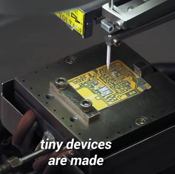
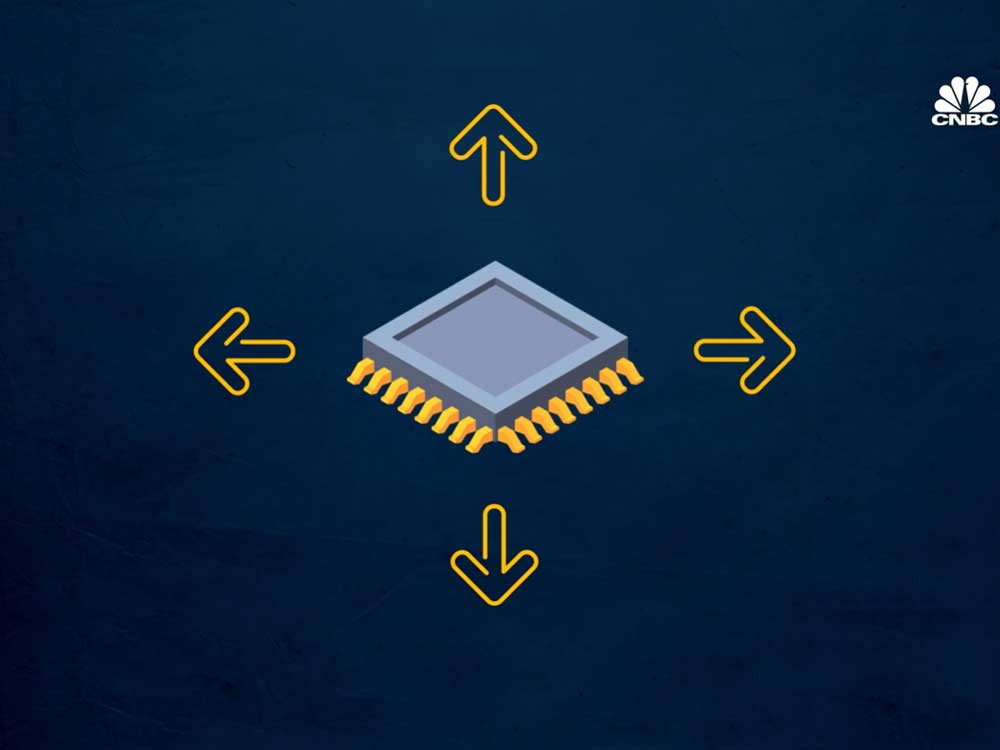
Aging test, also known as reliability enhancement test, is a method to test the performance stability and reliability of a product by simulating the extreme environmental conditions that a product may encounter in actual use.
This process involves strict control and monitoring of environmental factors such as temperature, humidity, vibration, etc., in order to accurately simulate the stress conditions that the product may encounter in actual applications.
Condition monitoring method of aging test process
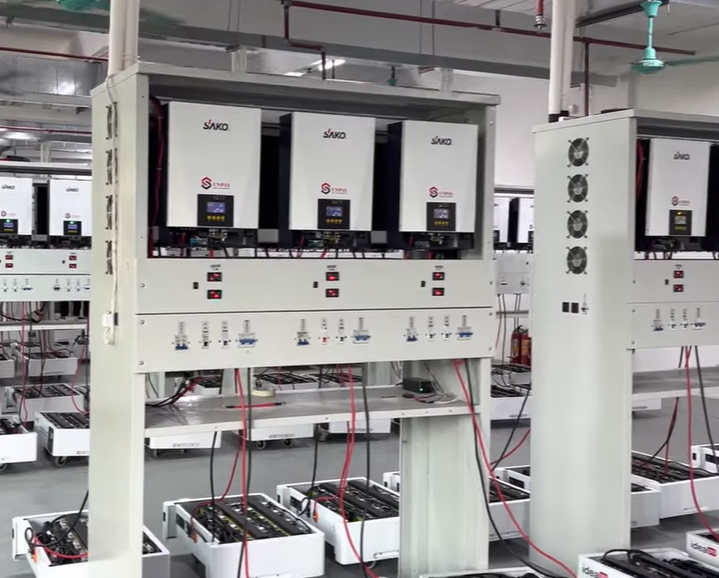
- Monitoring of environmental parameters: During the aging test process, monitoring of environmental parameters is crucial. This includes real-time monitoring of parameters such as temperature, humidity, air pressure, and lighting. By monitoring these parameters, the performance of the product under various environmental conditions can be effectively evaluated. Commonly used environmental parameter monitoring equipment includes temperature and humidity meters, barometers, light sensors, etc. These devices collect environmental parameter data in real time through sensor technology and transmit it to the computer through the data acquisition system for real-time analysis and recording.
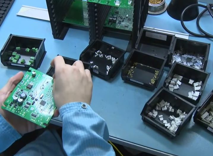
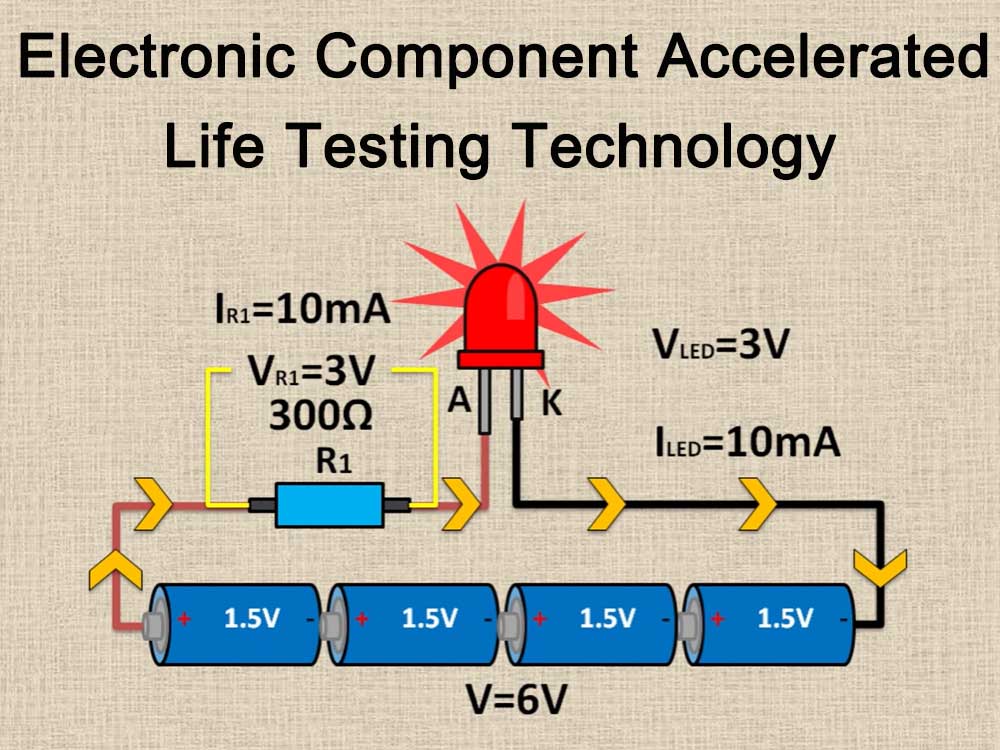
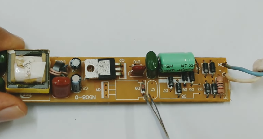
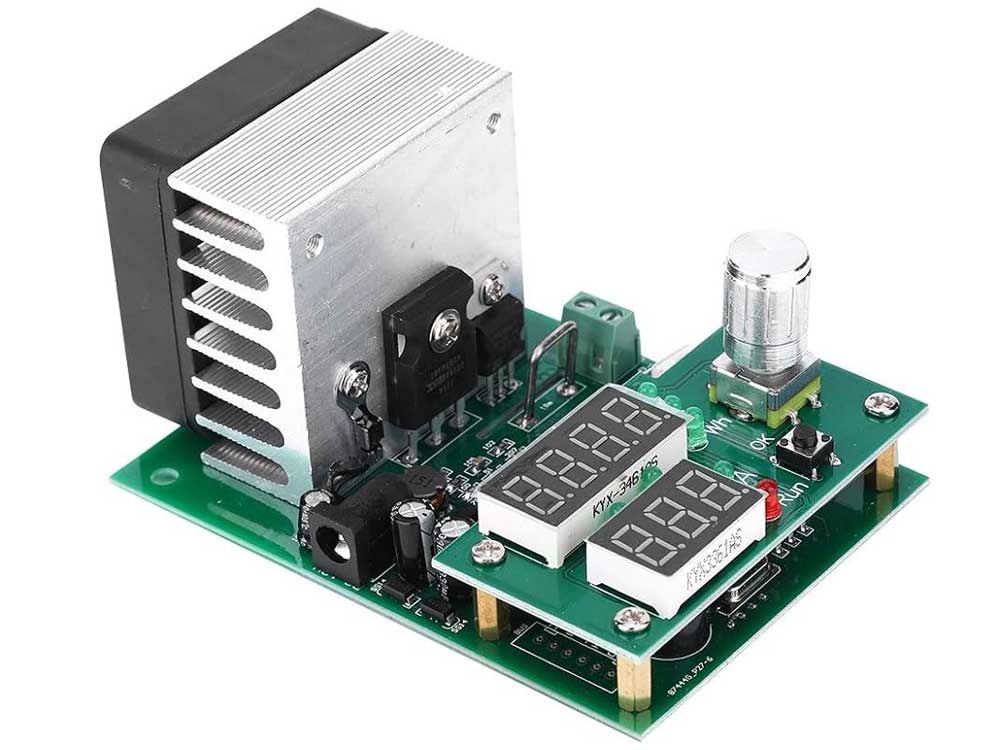
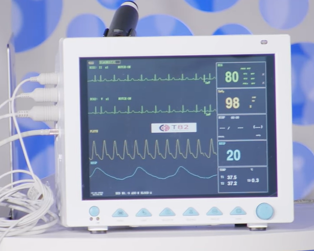
- Monitoring of product performance parameters: In addition to monitoring of environmental parameters, monitoring of product performance parameters is also an important part of the aging test. This includes monitoring of electrical performance parameters such as voltage, current, power, frequency, and waveform, as well as monitoring of product mechanical performance parameters such as vibration, shock, collision, etc. Through real-time monitoring of these performance parameters, we can understand the performance changes of the product during the aging test and thereby judge its reliability. Commonly used product performance parameter monitoring equipment includes oscilloscopes, spectrum analyzers, shaking tables, etc. These devices are connected through the interface with the product under test, and collect the performance parameter data of the product in real time, and transmit it to the computer through the data acquisition system for real-time analysis and recording.
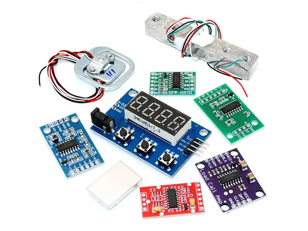
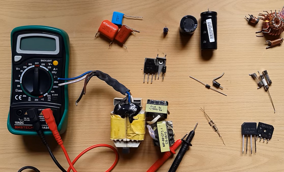
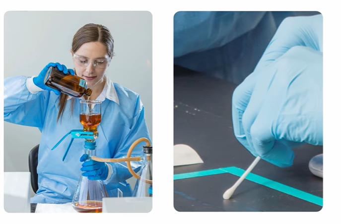
- Appearance and structural inspection: During the aging test, it is also necessary to inspect the appearance and structure of the product. This includes checking the product for obvious physical damage, deformation, leakage, etc. Inspection of appearance and structure can be carried out through visual inspection, touch inspection, etc. Non-destructive testing technologies such as X-ray testing, ultrasonic testing, etc. can also be used to further confirm the internal structure and integrity of the product.
- Data analysis and processing: During the aging test process, a large amount of data can be obtained through real-time monitoring of environmental parameters, product performance parameters, and appearance and structural inspection. The analysis and processing of these data is an important part of the aging test. Through data analysis and processing, the performance change trend of the product during the aging test can be understood, and the weak links and reliability issues of the product can be identified. Commonly used data analysis and processing methods include statistical analysis, trend analysis, fault diagnosis, etc. These methods can be implemented through various professional software such as MATLAB, Origin, etc.
In conclusion
Aging test is an important means to ensure the performance stability and reliability of electronic products or materials, and condition monitoring is a key part of the aging test.
Through real-time monitoring of environmental parameters, product performance parameters, appearance and structure, and in-depth analysis and processing of data, product reliability and potential problems can be more accurately assessed. In the future, with the development of sensor technology, data acquisition technology and analysis and processing technology, the condition monitoring of aging tests will be more accurate and efficient.
At the same time, methods based on artificial intelligence and machine learning will play an increasingly important role in fault prediction and intelligent diagnosis, further improving the accuracy and reliability of aging tests.
Frequently Asked Questions
Aging test, also known as reliability enhancement test, is a method to test the performance stability and reliability of a product by simulating the extreme environmental conditions that a product may encounter in actual use.
During the aging test process, real-time monitoring of the test status is the key to ensuring the accuracy and effectiveness of the test. By monitoring various parameters in real time, we can understand the performance of the product under various environmental conditions, judge its reliability, and discover and solve potential problems in a timely manner.
The condition monitoring methods of the aging test process mainly include environmental parameter monitoring, product performance parameter monitoring, appearance and structural inspection, and data analysis and processing. These methods can help obtain real-time data about a product, evaluate its performance, and identify potential problems.
Environmental parameter monitoring includes real-time monitoring of temperature, humidity, air pressure, light and other parameters. Commonly used equipment includes temperature and humidity meters, barometers, light sensors, etc., which collect data in real time through sensor technology and transmit it to the computer through the data acquisition system for real-time analysis and recording.
Product performance parameter monitoring involves the monitoring of electrical performance parameters such as voltage, current, power, frequency, waveform, etc., as well as the monitoring of product mechanical performance parameters such as vibration, impact, collision, etc. Commonly used equipment includes oscilloscopes, spectrum analyzers, shaking tables, etc., which are connected to the interface of the product under test to collect product performance parameter data in real time, and transmit it to the computer through the data acquisition system for real-time analysis and recording.
Inspection of appearance and structure includes visual inspection, touch inspection, etc., as well as the use of non-destructive testing technologies such as X-ray testing, ultrasonic testing, etc. to further confirm the internal structure and integrity of the product.
The large amount of data obtained through real-time monitoring requires in-depth analysis and processing. Commonly used methods include statistical analysis, trend analysis, fault diagnosis, etc. These methods can be implemented through various professional software such as MATLAB, Origin, etc.
With the development of sensor technology, data acquisition technology and analysis and processing technology, the condition monitoring of aging tests will be more accurate and efficient.
At the same time, methods based on artificial intelligence and machine learning will play an increasingly important role in fault prediction and intelligent diagnosis, further improving the accuracy and reliability of aging tests.