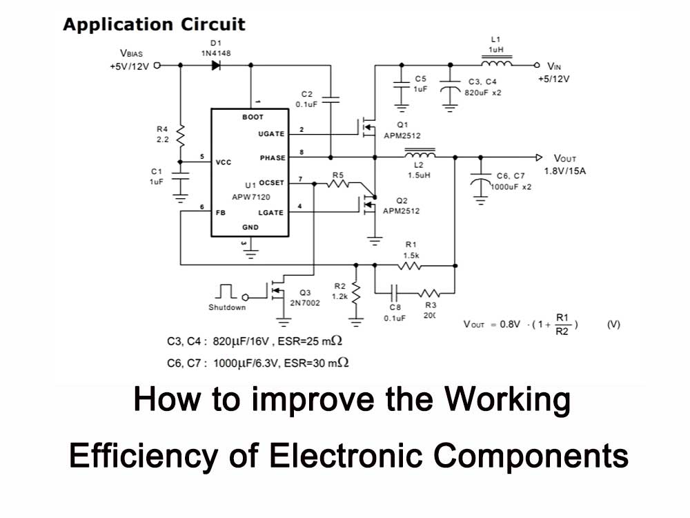
Improving the efficiency of electronic components is a complex problem involving many aspects. The efficiency of electronic components is mainly affected by factors such as design, manufacturing process, working environment and usage methods.
Here are some key strategies and methods that may help improve the efficiency of your electronic components:
Optimized design
Reduced Resistance: Reduce the resistance at the connection by improving the shape and material of the wire. For example, use thicker wires, adopt multi-layer circuit boards, implement surface mount technology, etc.
Increase integration: Improve the processing capabilities of electronic components by reducing feature size and increasing the number of transistors on the chip. This often relies on the development of Moore’s Law.
Thermal Design: Optimize the heat dissipation performance of components to prevent performance degradation caused by overheating. For example, you can add heat sinks, optimize heat dissipation channels, etc.
Improving New Manufacturing Technologies for Electronic Components
Nano manufacturing: Use nano-level manufacturing technology to reduce the size of components and improve their density and performance. For example, nanowires, nanofilms, etc.
New materials: Use new materials with higher conductivity, heat resistance or other superior properties, such as graphene, gallium nitride, etc.
Working environment optimization
Temperature Management: Ensure that electronic components do not overheat when working. This can be achieved through heat dissipation equipment, controlling the operating temperature range, etc.
Power Management: Optimize power supply, ensure stable voltage and current supply, and prevent efficiency decline caused by excessive or small voltage or current.
Environment Control: Control the humidity, air pressure, dust, etc. of the working environment to reduce the impact of the external environment on component performance.
Programming and Algorithm Optimization
Algorithm Improvement: Use more efficient algorithms and data processing technology to reduce computing time and resource consumption.
Parallel processing: Utilize multi-core processors or other parallel processing architectures to speed up data processing.
Code Optimization: Improve code execution efficiency by reducing redundant calculations and using appropriate data structures and algorithms.
Regular Maintenance: Check and clean electronic components regularly to ensure they are working properly.
Firmware/Software Updates: Timely update the firmware or software of electronic components to improve their performance and fix possible efficiency issues.
Reliability Design
Redundant Design: Improve the reliability of components by adding backup systems or components and reduce the overall efficiency decline caused by the failure of a single component.
Durability Test: Durability and reliability testing is performed during the production stage to ensure that components maintain high efficiency during the expected working life.
Energy Management
Sleep mode and wake-up mechanism: When electronic components are not working, put them in sleep mode to save energy and wake up quickly through appropriate mechanisms.
Energy-saving technology: Use energy-saving technologies such as switching power supplies to reduce energy consumption.
System integration and optimization
Integrate and optimize the work of multiple components at the system level to avoid wasting resources or reducing unnecessary energy consumption.
Other Strategies
Innovative Design: Encourage design innovation and explore new working principles and methods to improve the working efficiency of electronic components.
Personnel training: Provide training to personnel who operate and maintain electronic components to ensure that they understand how to optimize the working efficiency of components.
Continuous Research and Development
Continuously track and study new technological trends and developments in order to promptly adopt new methods and technologies that can improve the working efficiency of electronic components.
In short, improving the working efficiency of electronic components requires comprehensive consideration from many aspects, including design, manufacturing, working environment, usage methods, etc.
This is a multidisciplinary field that requires engineers to continuously explore and innovate in theory and practice.
With the continuous development of new technologies, more new methods to improve the working efficiency of electronic components are expected to emerge in the future.
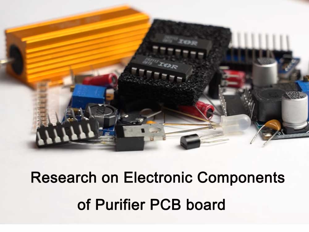
The research on electronic components of purifier PCB boards is dedicated to in-depth exploration of the role and working principle of electronic components in purifier PCB boards to improve the performance and stability of purifiers.
Through continuous technological innovation and market research, we continue to promote the progress of the purifier industry and provide users with more efficient and reliable products.
Purifier PCB circuit board refers to the PCB board used in purification machines. Its main function is to adsorb, decompose or transform various air pollutants, effectively improving air cleanliness.
Purifier PCB circuit board is an electronic component used in air purifiers. Its function is to control the operation of the air purifier and ensure that it works safely and effectively.
What electronic components does the purifier PCB circuit board consist of
PCB Board Components – Installing electronic components on a PCB board
Purifier PCB circuit board usually consists of the following electronic components:
Microcontroller: used to control and manage various functions and operations of the purifier.
Sensor: used to detect and monitor pollutant concentration, temperature, humidity and other parameters in the air.
Driver: used to control the drive circuit of fans, motors or other actuators to achieve functions such as wind speed adjustment and filter replacement of the air purifier.
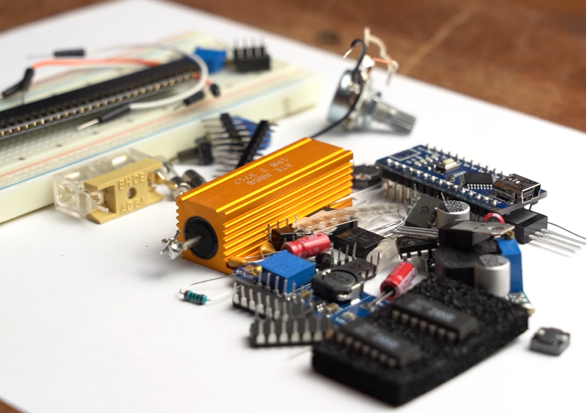
Circuit board: composed of pads, vias, mounting holes, wires, components, connectors, fillers, electrical boundaries, etc.
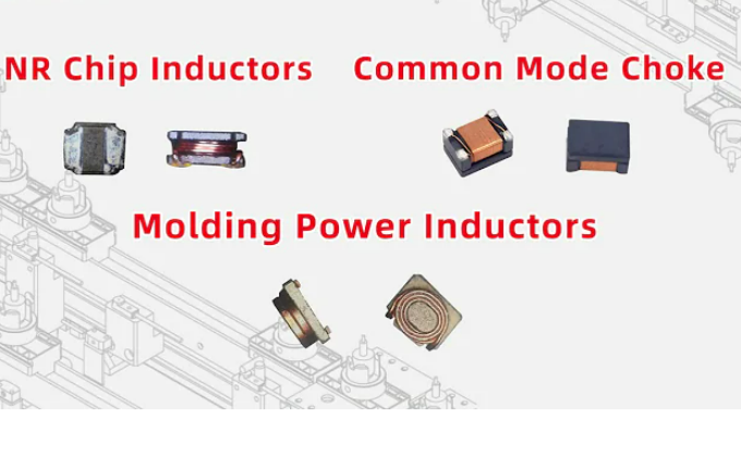
In addition, depending on actual needs, other electronic components may also be included, such as fuses, negative temperature coefficient resistors, common mode chokes, etc. These electronic components cooperate with each other to realize the functions of the purifier PCB circuit board.
How do the components of the purifier PCB circuit board work?
The electronic components on the purifier PCB circuit board cooperate with each other to realize various functions of the purifier.
As the core control unit, the microcontroller adjusts the speed of the fan or motor through the driver according to the detection results of the sensor to adjust the air flow and purification speed. At the same time, the microcontroller is also responsible for controlling various protection circuits and indication circuits to ensure the safe operation of the purifier and user convenience.
The sensor is used to monitor parameters such as pollutant concentration, temperature, and humidity in the air, and convert these parameters into electrical signals and transmit them to the microcontroller. The microcontroller determines the pollution of the air based on the received electrical signal and adjusts the output of the driver to achieve automatic control of air purification.
The driver controls the operation of fans, motors or other actuators according to instructions from the microcontroller. For example, when the air pollution level exceeds the standard, the driver will increase the fan speed to increase the air purification speed; when the air humidity is too high, the driver will activate the dehumidification function to reduce the air humidity.
Components include resistors, capacitors, diodes, transistors, integrated circuits, etc., which respectively implement the current limiting, filtering, rectification, amplification and other functions of the circuit to ensure the normal operation of the purifier circuit.
As a carrier to support and connect electronic components, the circuit board provides electrical connections such as wires and connectors to realize signal transmission and control between electronic components.
To sum up, the electronic components on the purifier PCB circuit board cooperate and control each other to complete various functions of the purifier and improve the quality of indoor air.
Which component controls and manages the purifier PCB circuit board?
The control and management of the purifier PCB circuit board is mainly responsible for the microcontroller (MCU). The microcontroller is the core control unit of the purifier. It is responsible for receiving and processing the signals input by the sensor. According to the set algorithms and programs, it controls the work of the driver and other actuators to realize various functions of the purifier, such as automatic detection and automatic adjustment. , intelligent control, etc. The microcontroller achieves precise control of the working process of the purifier through programs to ensure the performance and stability of the purifier. At the same time, the microcontroller can also realize communication and control with other smart home devices, making it convenient for users to perform remote control and intelligent management.
Which part of the purifier PCB is the most expensive?
The price of purifier PCB circuit boards varies depending on factors such as manufacturer, quality, function, and material, so it is impossible to generalize which part is the most expensive.
However, generally speaking, as the core control unit of a purifier, the price of a microcontroller is relatively high because it needs to have a high degree of reliability and stability to ensure the normal operation of the purifier.
In addition, components such as sensors and drivers are also relatively expensive parts because they need to accurately detect and regulate various parameters in the air.
Detailed introduction to the purifier PCB circuit board
Purifier PCB circuit board definition
*PCB, which stands for Printed Circuit Board, is an important electronic component. It provides electrical connections between various electronic components in electronic equipment.
PCBs allow electronic components to conductively connect to each other by creating conductive paths on thin sheets of material (such as epoxy, paper phenolic, etc.).
In air purifiers, the purifier PCB circuit board is the core component specially designed to control the functions of the air purifier. It integrates functional modules such as control, display, sensing and power supply to ensure the normal operation of the purifier.
How does the purifier PCB board work
The purifier PCB circuit board detects parameters such as air quality and pollutant concentration by receiving signals from sensors.
Based on these parameters, the purifier PCB circuit board controls the purifier’s operating mode, wind speed and working time.
It is also responsible for monitoring the status of the purifier, ensuring its normal operation, and providing alarm or shutdown functions when necessary to protect the equipment from damage.
Purifier PCB board components
Input part: receives external input signals, such as switch control signals, sensor detection signals, etc.
Processing part: Process the received signal and control the output signal according to the preset program.
Output part: Control the working status of each component according to the processed signal, such as motor, heating element, indicator light, etc.
Integrated components: including microcontrollers, transistors, resistors, capacitors and other electronic components, used to realize the logic and computing functions of the circuit.
Purifier PCB circuit board features
Efficient performance: The purifier PCB circuit board has efficient processing capabilities and can quickly respond to various instructions and sensor signals.
Strong stability: The circuit board design takes into account long-term operation and high load conditions, and has high stability and reliability.
Easy to maintain: Designed with repair and replacement needs in mind, the circuit board is easy to disassemble and replace damaged components.
Purifier PCB board application scenarios
Purifier PCB circuit boards are widely used in various types of air purifiers, such as household, commercial and industrial air purifiers.
As people’s attention to indoor air quality continues to increase, the demand for purifier PCB circuit boards is also gradually increasing.
Purifier PCB circuit board development trends
Intelligent: With the development of the Internet of Things and artificial intelligence technology, the purifier PCB circuit board will further realize intelligent functions, such as optimizing the operating mode of the air purifier through artificial intelligence algorithms, and realizing remote monitoring and control.
Integration: In order to simplify the design and production process of air purifiers, purifier PCB circuit boards may tend to have a higher level of integration, integrating more functions on one circuit board.
Environmentally friendly materials: With the increase in environmental protection requirements, more environmentally friendly materials may be used in the PCB manufacturing process to reduce the burden on the environment.
Purifier PCB precautions
When using and maintaining the purifier, safety operating procedures should be followed to avoid safety accidents such as electric shock due to improper operation.
Discarded purifier PCB circuit boards should be recycled and processed in accordance with relevant environmental protection regulations to avoid harm to the environment.
As the core component of the air purifier, the purifier PCB circuit board plays an important role in ensuring the normal operation of the air purifier and providing good indoor air quality.
As technology continues to advance and application demands continue to grow, purifier PCB circuit boards will continue to develop and achieve more functions and optimizations.
Globalbestshopping.com is a distributor, manufacturer, and wholesaler of electronic components in China. Tongsha is also an agent for a major electronic component brand.
Purifier PCB circuit board electronic components supplier is committed to providing high-quality, reliable electronic components to meet customer needs in the field of purifier PCB circuit boards.
We have rich industry experience and a professional technical team to ensure that we provide you with high-quality products and services.
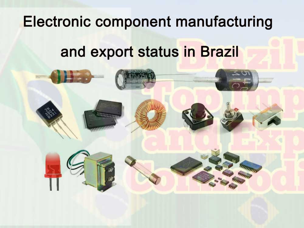
The export scale of Brazilian electronic component manufacturing plants continues to expand and has become an important part of the country’s export trade.
According to data released by the Brazilian government, Brazil’s exports of electronic components have continued to grow in recent years, showing a strong growth trend.
This growth trend reflects the increasing competitiveness of Brazilian electronic component manufacturing plants in the international market.
Brazil’s main export markets for electronic components
The main export markets for Brazilian electronic component manufacturing plants include Europe, Asia and North America. Europe is Brazil’s largest export market for electronic components. The main reason is that Europe’s electronic product manufacturing industry is developed and there is a large demand for high-quality electronic components.
The Asian market is another major export destination for Brazilian electronic components, especially emerging economies such as China and India. Their rapidly developing electronic product manufacturing industries provide a broad market space for Brazilian electronic components.
The North American market also has a large demand for Brazilian electronic components, especially the United States, whose large electronic product consumer group provides a stable source of demand for Brazilian electronic components.
Brazilian electronic component manufacturing plants export a wide range of products, including resistors, capacitors, diodes, transistors, integrated circuits, etc. These components are widely used in communications, consumer electronics, industrial control, automotive electronics and other fields. As Brazil’s electronic component manufacturing technology continues to improve, the types of export products are also constantly expanding to meet the diverse needs of the international market.
Competitive advantages and challenges of Brazilian electronic components
Brazilian electronic component manufacturing factories have certain competitive advantages in the international market. First, Brazil has abundant natural resources and low labor costs, making the production cost of electronic components relatively low. Secondly, with the continuous introduction of technology and accumulation of experience, the production process and technical level of Brazilian electronic component manufacturing plants have been significantly improved, and they are able to produce high-quality, high-reliability products.
In addition, in order to develop the international market, Brazilian electronic component manufacturing factories actively carry out international cooperation and establish cooperative relationships with well-known international companies, further enhancing the visibility and competitiveness of their products.
However, Brazilian electronic component manufacturing plants also face some challenges in the international market.
First of all, competition in the international market is fierce, especially from countries such as China and Japan. Secondly, the technology gap remains a major bottleneck for Brazilian electronic component manufacturing plants, especially in the field of high-end products.
In addition, changes in the international trade environment also have an important impact on the export of Brazilian electronic component manufacturing plants. For example, an increase in tariffs may increase export costs, while the signing of international trade agreements may bring more export opportunities to factories.
Future Prospects for Brazilian Electronic Components
In the future, with the continuous development and technological advancement of the global electronic product manufacturing industry, the export prospects of Brazilian electronic component manufacturing plants will still be broad.
In order to achieve greater success in the international market, Brazilian electronic component manufacturing factories need to continue to increase investment in technology research and development and innovation, and improve the quality and technical content of their products.
At the same time, strengthening international cooperation and market expansion is also key. By cooperating with internationally renowned companies and brands and actively participating in international trade activities, Brazilian electronic component manufacturing factories are expected to further enhance the international visibility and competitiveness of their products.
There are several reasons for choosing Brazilian electronic component manufacturers: Quality assurance: Brazil’s electronic component manufacturing factories have made significant progress in recent years and have high-quality, high-reliability production capabilities. By choosing a Brazilian electronic component manufacturer, you can get quality assurance and meet the needs of various electronic product manufacturing. Cost advantage: Compared with some well-known international brands, the cost of Brazilian electronic component manufacturing factories is relatively low. This gives a certain cost advantage in choosing Brazilian electronic component manufacturers, which can reduce production costs and improve the competitiveness of products. Technical strength: Brazil’s electronic component manufacturing factories have continuously introduced and accumulated experience in technology, and have strong R&D and innovation capabilities. By choosing Brazilian electronic component manufacturers, you can get advanced technical support and solutions to meet various technical requirements. Stable supply capacity: Brazil’s electronic component manufacturing factories have stable supply capacity and can ensure timely delivery and stable production. This is very important for manufacturers that require a large number of electronic components to ensure the smooth progress of production. Diversified product types: Brazilian electronic component manufacturing factories are able to produce diversified product types to meet the needs of different customers. From resistors, capacitors, diodes to transistors, integrated circuits, etc., Brazil’s electronic component manufacturing factories can provide them to facilitate customers’ one-stop purchasing. In short, choosing Brazilian electronic component manufacturers can gain the advantages of quality assurance, cost advantages, technical strength, stable supply and diversified products. In the field of electronic product manufacturing, choosing the right electronic component manufacturer is crucial to product quality and competitiveness.
What is the level of manufacturing technology of electronic components in Brazil?
The manufacturing technology level of Brazilian electronic components has made certain progress in recent years, but compared with some developed countries, there is still a certain gap. This is mainly due to Brazil’s relative lag in basic research and innovation in the electronics industry, as well as the lack of sufficient technical talents and advanced production equipment. Despite this, Brazil’s electronic component manufacturing technology is still competitive in some areas. For example, in the fields of power electronics and embedded systems, some Brazilian companies have relatively advanced manufacturing technologies and are able to produce high-quality products. In addition, Brazil also has certain competitive advantages in certain specific markets, such as in the field of automotive electronics, where Brazilian electronic component manufacturers perform well in meeting local market demand. In order to improve the manufacturing technology level of electronic components, the Brazilian government and enterprises are taking a series of measures. For example, the Brazilian government has increased investment in the electronics industry, encouraging companies to strengthen technology research and development and innovation, while introducing advanced foreign technology and management experience. In addition, Brazilian companies are also actively carrying out technical cooperation and exchanges to improve their technical level and production efficiency. Generally speaking, the manufacturing technology level of electronic components in Brazil still needs to be improved, but through the joint efforts of the government and enterprises, I believe there will be more progress and innovation in the future.
Are Brazilian electronic components produced in-house?
Yes, Brazilian electronic components are mainly produced by Brazilian domestic electronic component manufacturers. These manufacturers produce a wide range of electronic components such as resistors, capacitors, diodes, transistors, etc. as per market demand and specific specifications. Brazil’s electronic components manufacturing industry has developed rapidly in recent years, and its technical level and production capacity have continued to improve. It can not only meet the needs of the domestic market, but also actively expand the international market. Brazil’s electronic component manufacturers are mainly concentrated in areas such as Sao Paulo and Rio de Janeiro. These areas have complete industrial chains and industrial clusters, providing favorable conditions for enterprise development. In addition, the Brazilian government has also introduced a series of policies to encourage the development of the electronic components manufacturing industry and provide more support and guarantees for enterprises. Despite this, there is still a technical gap between Brazil’s electronic components manufacturing industry and the international advanced level, especially in the field of high-end products. Therefore, Brazilian electronic component manufacturers are constantly increasing investment in technology research and development and innovation, and are striving to improve product quality and technical content to enhance their competitiveness in the international market.
What are the advantages of Brazil’s electronic components industry?
Brazil’s electronic components industry has the following advantages: Abundant natural resources: Brazil is rich in mineral resources, such as copper, iron, tin, etc. These resources are important raw materials required for the manufacturing of electronic components. Lower labor costs: Compared with some developed countries, Brazil’s labor costs are lower, which gives Brazilian electronic component manufacturing companies a certain competitive advantage in terms of cost. Strong market demand: The demand for electronic products in the Brazilian domestic market continues to grow, which provides a broad market space for electronic component manufacturing companies. Policy support: The Brazilian government has provided certain policy support to the manufacturing and electronic component industries, including tax incentives, financial support, etc., providing favorable conditions for industrial development. Technological progress: Brazilian electronic component manufacturing companies have continued to make technological progress, and their production processes and technical levels have continued to improve, improving product quality and competitiveness. To sum up, Brazil’s electronic components industry has certain advantages in terms of natural resources, labor costs, market demand, policy support and technological progress, which provides favorable conditions for industrial development.
How does Brazilian electronic component manufacturing technology compare with Japan?
Compared with Japan, there is a certain gap between the manufacturing technology of Brazilian electronic components. Japan has a high level of technology and rich experience in the manufacturing of electronic components. It has advanced production equipment and processes, and it also has high innovation capabilities in materials research and development and design. In contrast, Brazil’s basic research and innovation in electronic component manufacturing is relatively lagging behind, and its production equipment and processes are also relatively backward, which restricts the improvement of its technological level. In addition, Japan has a complete technical ecology and industrial chain in the electronics industry and can provide a full range of services and solutions. This is also an aspect that needs to be strengthened in Brazil’s electronic component manufacturing technology. Of course, Brazil also has certain technical advantages and characteristics in certain fields. For example, in the fields of power electronics and embedded systems, some Brazilian companies have relatively advanced manufacturing technologies and can produce high-quality products. Therefore, Brazil still needs to comprehensively improve its electronic component manufacturing technology level, while at the same time giving full play to its own advantages and characteristics and strengthening cooperation and technical exchanges with advanced international companies.
Which countries do Brazilian electronic component manufacturers mainly sell their products to?
The products of Brazilian electronic component manufacturers are mainly sold to the following countries: Domestic market: Brazilian electronic component manufacturers first meet the needs of the domestic market. With the development of Brazil’s electronic product manufacturing industry, the domestic market’s demand for electronic components continues to grow. European market: Europe is one of the important export destinations of Brazilian electronic components. Europe’s electronic product manufacturing industry is developed and there is a large demand for high-quality electronic components. Therefore, Brazilian electronic components have a certain market share in the European market. Asian market: Especially in emerging economies such as China and India, their rapidly developing electronic product manufacturing industries provide a broad market space for Brazilian electronic components. North American market: Especially the United States, its huge consumer group of electronic products provides a stable source of demand for Brazilian electronic components. Generally speaking, the products of Brazilian electronic component manufacturers are sold to many countries and regions around the world, mainly in areas with developed electronic product manufacturing industries. In the future, with the continuous development and technological advancement of the global electronic product manufacturing industry, the products of Brazilian electronic component manufacturers are expected to be sold to more countries and regions.
In which regions is the Brazilian electronic components industry mainly concentrated?
Brazil’s electronic components industry is mainly concentrated in the following regions: Sao Paulo and Rio de Janeiro: These two areas have large electronic markets that supply a variety of electronic components and products. In São Paulo, there are numerous electronics shops and markets near Paulista Avenue, supplying components, electronic equipment and accessories. Buenos Aires: Buenos Aires, the capital of Argentina, has a number of electronic markets and vendors offering electronic components and products. Vendors are located in places such as the city center and Herrera Avenue. Due to factors such as geographical location, economic conditions, and policy support, these areas have attracted a large number of electronic component manufacturing companies and investments, forming relatively complete industrial chains and industrial clusters, and promoting the development of Brazil’s electronic components industry.
This process requires delicate operating skills and strict quality control to ensure the long-term stability and reliability of the product.
LED PCB board introduction
LED PCB board, also known as LED light board or LED circuit board, is an important electronic component, mainly used to connect LED lamp beads with circuits to achieve lighting, display or other functions. LED PCB boards are usually made of insulating materials, such as FR4 or aluminum substrates, with conductive lines and mounting locations for LED lamp beads designed on them.
PCB Assembly Manual Soldering – Although we use machines as much as possible even for one off assemblies, yet we cannot avoid that for some boards, manual soldering is necessary. Manual soldering is not a task but an art! – Contact PCB Assembly Factory Now
Electronic components are the basic units that constitute electronic products, including resistors, capacitors, inductors, diodes, transistors, ICs, etc. In LED PCB boards, the following components are usually required:
LED lamp beads: used to generate light and are the core components of LED PCB boards.
Resistor: used to limit current and protect LED lamp beads from overcurrent damage.
Capacitor: used for filtering and decoupling to improve circuit stability.
Diode: used for rectification to ensure that the LED lamp beads work at the correct voltage.
IC: used to control circuit functions, such as driver IC, etc.
Choosing the right electronic components is crucial to the performance of the LED PCB board. The selection needs to be based on specific application requirements, working voltage, current, working environment temperature and other factors.
Assembly process of electronic components
Component inspection: Ensure that all components are intact and specifications meet design requirements.
PCB board cleaning: Use alcohol or cleaning agent to remove dirt and grease on the surface of the PCB board.
Apply flux: Apply an appropriate amount of flux on the PCB board wires that need to be welded.
Component placement: According to the design requirements, place the electronic components on the PCB board in the correct direction and position.
Welding: Use a soldering iron or a hot air gun to weld the components to the PCB board to ensure reliable welding quality.
Solder joint inspection: Check whether all solder joints are full and there are no empty solder joints or continuous solder joints.
Assembly quality inspection: Carry out functional testing and appearance inspection to ensure that the assembly quality meets the requirements.
Finished product packaging: Pack the qualified LED PCB boards for transportation and storage.
Things to note when assembling electronic components on LED PCB boards
During the welding process, the welding temperature and time must be controlled to avoid thermal damage to LED lamp beads and other components.
When welding, pay attention to the quality of the solder joints to avoid false soldering, continuous soldering, etc., which will affect the continuity and reliability of the circuit.
Keep it clean during the assembly process to avoid dust, dirt and other impurities from entering the inside of the PCB board and affecting the normal operation of the circuit.
Some sensitive components, such as ICs, crystal oscillators, etc., need to be handled with special care to avoid being affected by excessive mechanical stress or static electricity.
After assembly is completed, comprehensive quality inspection is required to ensure that the performance and reliability of the product meet the requirements.
LED PCB board electronic component assembly summary
Assembling electronic components on an LED PCB is a process that requires professional skills and experience. In order to ensure the quality and reliability of the product, it is necessary to select appropriate components, follow the correct assembly process, and pay attention to various precautions. Through continuous learning and practice, we can improve our skill levels and contribute to the production of high-quality LED PCB boards.
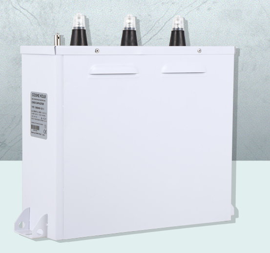
Cook Cooper Smart Capacitor Operation Guide: From installation to maintenance, we provide you with detailed operating guidance to ensure the safe and stable operation of the capacitor and effectively improve the performance of the power system.
Cook Cooper smart capacitor is a power electronic device used for reactive power compensation and filtering. It integrates modern power electronics technology and intelligent control algorithms, which can dynamically adjust reactive power and active power to improve the stability of the power system, reduce energy consumption and improve power quality.
This operating guide is intended to provide users with detailed operating guidance on Cook Cooper smart capacitors.
Cook Cooper Smart Capacitor Installation
Confirm the capacitor installation environment: Make sure the capacitor is installed in a dry, well-ventilated environment without severe vibration or corrosive gases.
Grounding: Reliably ground the metal shell of the capacitor to ensure safe operation.
Cable connection: Use appropriate cables to connect the capacitor to the system, making sure the connection is firm and not loose.
Inspection before operation: Check whether the capacitor wiring is correct and there is no short circuit, open circuit, etc.; check whether the appearance of the capacitor is intact and there is no damage, leakage, etc.
How a Capacitor Works – Capacitor Physics and Applications
Cook Cooper Smart Capacitor Operation
Put into operation: After confirming that the capacitor wiring is correct and the appearance is intact, put the capacitor into operation through the control switch.
Out of service: When the capacitor needs to be out of service, it is removed from the system through the control switch.
Parameter setting: According to actual needs, set parameters of the capacitor through controller or touch screen and other equipment, such as switching delay, compensation target, etc.
Troubleshooting: When an abnormality occurs in the capacitor, it should be stopped immediately and inspected and repaired. For faults that cannot be eliminated, it is recommended to contact professionals for repair.
Cook Cooper Intelligent Capacitor Maintenance
Regular inspection: Regularly inspect the capacitor, including whether the appearance is damaged, leaking, etc.; whether the wiring is loose; whether the control equipment is normal, etc.
Cleaning and maintenance: Keep the capacitor and its surrounding environment clean, and regularly clean up dust and other debris to ensure good heat dissipation.
Preventive tests: Conduct preventive tests regularly according to actual conditions, such as measuring insulation resistance, withstand voltage tests, etc., to ensure normal performance of the capacitor.
Life assessment: Evaluate the life of the capacitor based on its operating conditions, and replace aging or damaged capacitors in a timely manner.
Precautions for Cook Cooper Smart Capacitors
Safe operation: When operating capacitors, safety procedures should be followed to ensure that operators have appropriate electrical knowledge and operating skills.
Overloading is prohibited: Avoid long-term operation exceeding the rated current of the capacitor to avoid equipment damage or safety accidents.
Frequent switching is prohibited: Avoid frequent switching of capacitors to avoid unnecessary impact on the equipment.
Regular calibration: Calibrate the control equipment regularly to ensure that its measurement and adjustment accuracy meets the requirements.
Keep records: Record the operation and maintenance of capacitors to facilitate tracking and management of the status of the equipment.
Common faults of capacitors and their troubleshooting methods
Abnormal noise from the capacitor: It may be caused by internal component failure or poor contact. It should be stopped immediately and inspected and repaired.
Capacitor overheating: It may be caused by excessive operating current or poor heat dissipation. The operating current should be reduced or the heat dissipation conditions should be improved.
Control equipment failure: It may be caused by equipment failure such as controllers and sensors. Relevant equipment should be inspected and repaired or replaced.
No compensation effect: It may be caused by incorrect wiring, improper setting of control equipment or mismatched capacitor bank. Relevant equipment and wiring should be checked, parameter settings should be re-set or capacitor bank configuration should be adjusted.
Conclusion on Cook Cooper Smart Capacitors
This operating guide is intended to provide users with detailed operating guidance on Cook Cooper smart capacitors, to help users correctly use and maintain the equipment, and to ensure its safe and stable operation.
If you encounter problems during use, you can refer to this guide for troubleshooting and processing; if you cannot solve the problem, please contact professionals for repair and processing.
Reliability research on DC/DC power modules is a multi-faceted topic that requires analysis from multiple perspectives such as module principles, applications, environmental factors, and failure modes.
The following is a brief research report summary designed to provide an in-depth understanding of this topic.
Introduction to DC/DC module reliability research
As a key component of power conversion, DC/DC power modules are widely used in various electronic equipment.
How Boost Converters Work (DC-DC Step-Up) – Electronics Intermediate 1
Due to their compact size, high efficiency and high reliability, DC/DC power modules have become the first choice for many applications. However, as the complexity of electronic equipment increases, the reliability problem of power modules becomes more and more prominent. Therefore, it is of great practical significance to study the reliability of DC/DC power modules.
DC/DC power module is a power supply that converts DC input voltage into DC output voltage. Its working principle mainly includes two processes: voltage conversion and current control. Voltage conversion is achieved through switching tubes and magnetic components (such as transformers and inductors), while current control is achieved through error amplifiers and feedback loops.
Factors affecting the reliability of DC/DC power modules
Component aging: Components in the power module, such as switching tubes, magnetic components and capacitors, will gradually age with time, affecting the reliability of the module.
Environmental factors: Environmental factors such as ambient temperature, humidity, vibration, and electromagnetic interference will also affect the reliability of the power module.
Load characteristics: The load characteristics of the power module, such as the size and change of the load current, also have an important impact on the reliability of the power module.
Design and manufacturing process: The design and manufacturing process of the power module also have a great impact on its reliability. Reasonable circuit design, high-quality components and strict manufacturing processes can improve the reliability of power modules.
Use and maintenance: Improper use and maintenance will also affect the reliability of the power module. For example, excessive use, lack of regular cleaning and maintenance, etc.
Methods to improve the reliability of DC/DC power modules
Choose high-quality components: Choosing high-quality components can effectively improve the reliability of the power module.
Optimize circuit design: Optimizing circuit design can improve the stability and efficiency of the power module, thereby reducing the failure rate.
Enhanced heat dissipation design: Enhanced heat dissipation design can prevent the power module from overheating, thereby reducing the aging rate of components.
Improve the level of manufacturing technology: Improving the level of manufacturing technology can reduce damage to components during the manufacturing process, thereby improving the reliability of the power module.
Implement regular maintenance: Regular inspection and maintenance of the power module can detect and solve potential problems in time, thus improving its reliability.
Choose a suitable application environment: Understanding and choosing a suitable application environment can prevent power module failures caused by environmental factors.
Properly select and use loads: Understanding and rationally selecting and using loads can prevent power module failures caused by load problems.
Enhance the maintainability of the power module: Considering the maintainability of the power module during the design stage can reduce troubleshooting and repair time during later use, thereby improving its reliability.
How to design DC/DC power module to improve its reliability
To improve the reliability of DC/DC power modules, you can start to consider it from the design stage. Here are some design tips:
Redundant design: In situations with high reliability requirements, even if the power module is damaged, the system cannot be powered off. At this time, redundant power supply can be used to improve system reliability. When one power module is damaged, the other module can continue to provide power.
Temperature Management: Properly arrange radiators, fans and other cooling devices to ensure that the module works within a suitable temperature range, which can reduce the failure rate.
Electromagnetic compatibility design: Ensure that the module has good anti-interference ability and avoid electromagnetic radiation and electromagnetic susceptibility interference. For example, the input and output ends of the module need to be filtered and isolated.
Voltage margin design: Set a reasonable margin for the operating voltage, and consider voltage fluctuations and ripple factors in module design to prevent power supply collapse.
Protection measures: Use overvoltage, overcurrent and overheating protection circuits to prevent the module from being damaged under extreme working conditions.
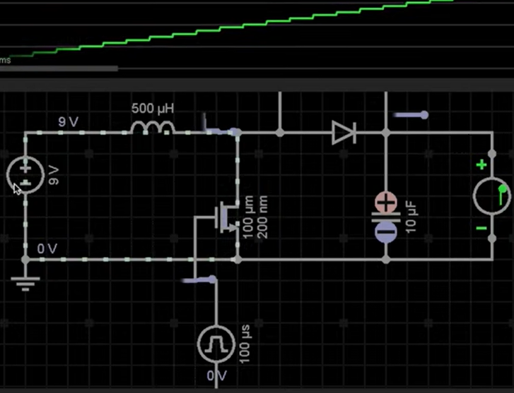
Unbalanced dual-channel power and voltage output design: For modules with unequal output power, there are two main design methods: one is to use transformer windings and use coupled inductors and low-voltage stabilizing circuits Perform secondary voltage stabilization method. The second is to use multiple secondary windings of the transformer to output two relatively independent voltages. Although method one can improve the stability of the circuit and ensure the accuracy of the output voltage, it will increase the loss of the circuit. If method 2 is adopted, since the feedback can only control one voltage, the accuracy of only one output voltage can be guaranteed. The voltage of the other voltage can only be pre-stabilized by the transformer and filter inductor, and the main output power will inevitably change greatly. It brings about large changes in the secondary voltage of the auxiliary circuit transformer, so the accuracy of the output voltage cannot be guaranteed. To this end, this design uses two outputs for independent control and feedback, so that the output voltage can be accurately controlled and the losses caused by secondary voltage stabilization can be reduced.
Derating design: When the power supply is fully loaded for a long time, its service life will be shortened. The derating design can effectively increase the service life of the power supply. The high-energy cubic ACDC module power supply is recommended to be used within the load range of 30%~80% for the best performance in all aspects.
Peripheral protection design: Reasonable design can protect the power module from the external environment. For example, appropriate filter circuits or capacitors can be added to reduce ripple noise or improve power supply stability.
These design techniques can improve the reliability of DC/DC power modules to a certain extent, but it should be noted that each application scenario has its own unique environment and requirements, so selections need to be made based on the actual situation during the specific design process. and applications.
DC/DC power module reliability conclusion
The reliability of DC/DC power modules is crucial to their wide application. From component selection, circuit design, manufacturing process to use and maintenance, all aspects need to be fully considered and effective strategies implemented to improve its reliability.
With the continuous development of science and technology, we also need to continue to conduct in-depth research on new technologies and methods to further improve the reliability of DC/DC power modules and meet the growing demand for electronic equipment.
The selection of electronic components in aerospace electronic systems is a complex and important task because it directly affects the performance, reliability and life of the spacecraft.
In the aerospace field, electronic components must be able to withstand extreme environmental conditions, such as high vacuum, strong radiation, high and low temperatures, etc., while also having the characteristics of high precision, high stability and long life.
Therefore, when selecting electronic components, in-depth analysis and consideration are required from many aspects.
Working principle and circuit design
In aerospace electronic systems, the working principles and circuit design of electronic components are crucial. First of all, it is necessary to consider whether the working principle of the electronic components meets the needs of the system, such as whether it has the required amplification, filtering, switching and other functions. Secondly, the circuit design also needs to be carefully considered, including the layout of components, connection methods and electromagnetic compatibility. In design, it is necessary to follow the principle of simplicity and reduce the number and complexity of components as much as possible to improve the reliability and stability of the system.
Environmental adaptability
Spacecraft will experience various extreme environmental conditions during launch, operation and recovery, such as high vacuum, strong radiation, extreme temperatures, etc. Therefore, the selected electronic components must have the ability to adapt to these environmental conditions. For example, the materials, structure, and packaging of components must be able to withstand the effects of vacuum and radiation environments; at the same time, the electrical performance of components needs to remain stable at extreme temperatures. In addition, the impact of other environmental factors such as humidity, salt spray and mold on components needs to be considered.
Reliability and longevity
Aerospace electronic systems have very strict requirements on reliability and lifespan. Therefore, the selected electronic components must have high reliability and long life. When selecting components, it is necessary to evaluate their reliability, including failure rate, mean time between failures, and failure prediction. At the same time, the lifespan of components also needs to be predicted and evaluated to ensure the long-term normal operation of the spacecraft. In order to improve the reliability and life of components, some measures can be taken, such as derating, redundant design and protective measures.
Performance and precision
Aerospace electronic systems also have very high requirements for performance and accuracy. Therefore, the electronic components selected must have high performance and precision. When selecting components, it is necessary to conduct a detailed understanding and analysis of their performance parameters to ensure that they meet the needs of the system. At the same time, the accuracy of components also needs to be evaluated and controlled to ensure the stability and accuracy of the system. In order to improve the performance and accuracy of components, some measures can be taken, such as selecting appropriate materials and processes, conducting accuracy testing and control, etc.
Maintainability and replaceability
Electronic components in aerospace electronic systems must be maintainable and replaceable so that they can be repaired and replaced in a timely manner in the event of failure. Therefore, when selecting electronic components, you need to consider the ease of maintenance and replacement, and give priority to standardized and universal components. In addition, in order to facilitate maintenance and replacement, methods such as modular design can also be used to divide the system into several independent modules, and each module can be repaired and replaced independently.
Cost and resource utilization
The cost of aerospace electronic systems is one of the factors that must be considered. When selecting electronic components, you need to consider their cost and resource utilization. On the premise of meeting system requirements, give priority to components with reasonable prices and sufficient resources. In addition, in order to reduce costs and improve resource utilization efficiency, some measures can also be taken, such as optimizing design solutions and improving production efficiency.
Technology and market development
With the continuous advancement of science and technology and the development and changes of the market, the technology and market of electronic components are also constantly developing and changing. Therefore, when selecting electronic components, you need to consider their technological maturity and market development trends. Prioritize components with high technological maturity and good market prospects to reduce risks and improve competitiveness. At the same time, it is also necessary to pay attention to the dynamics of new technologies and new products in order to make timely adjustments and innovations.
To sum up, the selection of electronic components in aerospace electronic systems requires comprehensive consideration of multiple factors.
In specific operations, it is necessary to conduct in-depth analysis and research according to the needs and characteristics of the system, select the most suitable electronic components and carry out reasonable application and maintenance.
At the same time, it is necessary to constantly pay attention to the development trends of technology and market to maintain the leading position and competitiveness of aerospace electronic systems.
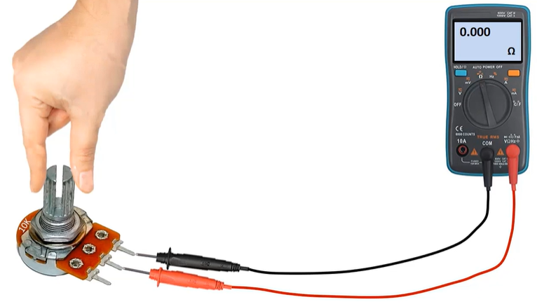
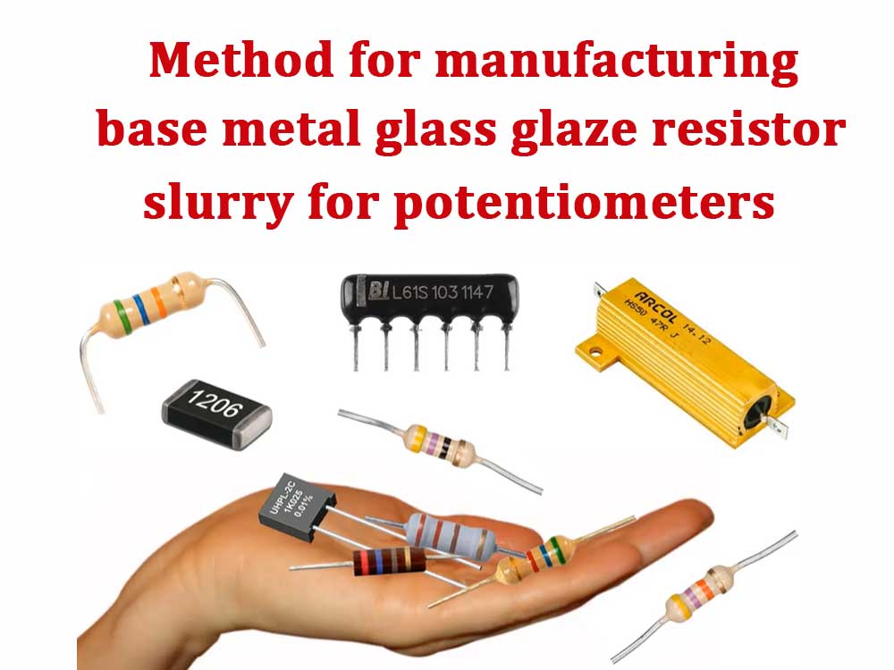
A potentiometer is an adjustable electronic component widely used in electronic equipment. Base metal glass glaze resistor slurry is an important material in potentiometer manufacturing, and its performance directly affects the quality and stability of the potentiometer.
This article will introduce in detail the manufacturing method of base metal glass glaze resistor slurry for potentiometers, including raw material selection, batching, mixing, grinding, modulation, filtration, inspection and packaging.
Raw material selection
Base metal powder: Choose base metal powder with high purity, uniform particle size and stable resistivity, such as nickel, chromium, copper, etc. These metals have good electrical conductivity and stability and can meet the requirements of potentiometers.
Glass glaze: Glass glaze is an inorganic non-metallic material with high temperature stability, chemical stability and good insulation properties. To select a glass glaze suitable for potentiometers, it is required that its composition has good compatibility with the base metal powder and can form a dense resistive film during the sintering process.
Organic carrier: Organic carrier is an important component of resistor slurry, which plays the role of dispersing metal powder and glass glaze and adjusting the viscosity of the slurry. Choose organic carriers with moderate volatility and good environmental performance, such as terpineol, butyl carbitol, etc.
Ingredients
Base metal powder, glass glaze and organic carrier are mixed according to a certain proportion. The proportion of ingredients is adjusted according to the performance requirements and manufacturing process of the potentiometer.
Generally speaking, the higher the content of base metal powder, the lower the resistivity; the higher the content of glass glaze, the higher the resistivity.
mix
Put the prepared raw materials into the mixing equipment and mix them so that the base metal powder, glass glaze and organic carrier are fully and evenly mixed together. The mixing time and speed should be moderate to avoid agglomeration of metal powder and excessively large glass glaze particles.
Grind
The mixed slurry needs to be ground to reduce the particle size and improve the fineness and uniformity of the slurry. Grinding equipment can use ball mills, sand mills, etc. During the grinding process, the grinding time and the type and quantity of grinding media should be controlled to avoid excessive grinding that will lead to a decrease in slurry performance.
modulation
The ground slurry needs to be modulated to adjust the viscosity and fluidity of the slurry. Appropriate amounts of diluents, thickeners and other auxiliary materials can be added during the preparation process. The prepared slurry should have good brushability and adhesion to form a uniform resistance film on the potentiometer substrate.
filter
The prepared slurry needs to be filtered to remove impurities and particles. Filtration equipment can use wire mesh filters, filter cloth filters, etc. The filtered slurry should be clean and free of impurities to ensure the quality and stability of the potentiometer.
test
Conduct quality inspection on the filtered slurry, including appearance, viscosity, fineness, solid content, resistivity and other indicators. Only the slurry that has passed the inspection can be packaged and used. Unqualified slurry needs to readjust the proportion of ingredients or undergo other processing until it meets the quality requirements.
Package
The slurry that has passed the inspection should be packaged in containers with good sealing, corrosion resistance, non-toxic and odorless packaging materials. During the packaging process, long-term contact between the slurry and the air should be avoided to avoid volatilization of the organic carriers in the slurry causing performance changes. The packaged slurry should be marked with product name, batch number, production date and other information to facilitate traceability and management.
Summary and Outlook
This article introduces in detail the manufacturing method of base metal glass glaze resistor slurry for potentiometers, including the steps of raw material selection, batching, mixing, grinding, modulation, filtration, inspection and packaging. These steps are of great significance to ensure the quality and stability of the potentiometer.
In the future, with the advancement of science and technology and the development of the market, the performance requirements for base metal glass glaze resistor slurries used for potentiometers will become higher and higher, and the manufacturing methods will also be continuously optimized and improved.
By adopting new raw materials, optimizing process flow, improving automation and other measures, more efficient, environmentally friendly and more stable manufacturing of base metal glass glaze resistor slurries for potentiometers can be achieved.
Metallic Glass Glaze Resistors and Potentiometers FAQ
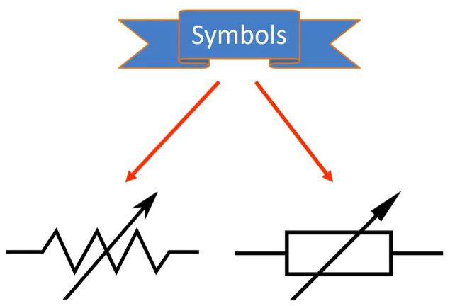
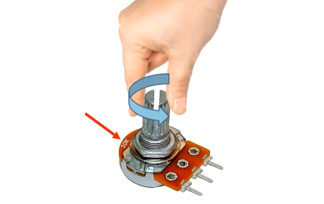
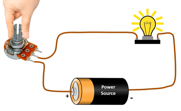
What is a potentiometer?
A potentiometer is an adjustable electronic component used to adjust the voltage or resistance value in a circuit. It usually consists of a resistor and a movable brush. The brush changes the resistance of the resistor by rotating or sliding, thereby adjusting the voltage or resistance value in the circuit. Potentiometers are widely used in various electronic devices, such as volume adjustment, brightness adjustment, power switches, etc. Depending on the application requirements, potentiometers can be divided into wirewound potentiometers, carbon film potentiometers, photosensitive potentiometers and other types.
What is a linear potentiometer?
A linear potentiometer is a special potentiometer whose resistance changes linearly with the movement of the slider. Linear potentiometers are often used in applications that require precise control of voltage or current, such as audio equipment, analog circuits, etc. Because its resistance value changes linearly, it can provide smooth adjustment effect and has a wide adjustment range. The accuracy and stability of linear potentiometers are key factors affecting their performance, so precise control and testing are required during the manufacturing process.
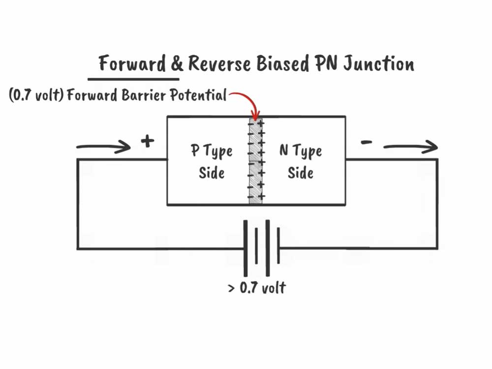
What is a glass resistor?
Glass resistor is a fixed resistor, usually composed of a metal conductor and a layer of glass. The glass is evenly coated on the surface of the resistor core through special process technology to form a protective layer, so that the resistor has good insulation properties. The working principle of glass resistors is based on Ohm’s law, which states that at a certain voltage, the current is proportional to the resistance. When electricity flows through a glass resistor, the electrons experience resistance, creating heat. This power conversion can be expressed as P=VI or P=I²R. Glass resistors mainly play a role in limiting current in circuits. They can be designed to limit voltage, control current, and measure electrical signals. At the same time, due to its high temperature resistance, corrosion resistance, moisture resistance and other characteristics, glass resistors are often used as circuit regulators, power filters and test components of various instruments and equipment.
How does a glass resistor work?
The working principle of glass resistors is based on Ohm’s law, which states that at a certain voltage, the current is proportional to the resistance. When electricity flows through a glass resistor, the electrons experience resistance, creating heat. This power conversion can be expressed as P=VI or P=I²R. In a glass resistor, the glass acts as a medium to insulate and isolate, and the metal conductor acts as a resistor. When current passes through the metal conductor and the glass layer, the current is blocked due to resistance, causing the electrons in the metal conductor to slow down in the glass layer, thus producing resistance. The resistance value of a glass resistor will also vary due to the different resistivities of the metal conductors, as well as the thickness and uniformity of the glass layer. Therefore, by controlling parameters such as the material, shape and size of the metal conductor, as well as the thickness and uniformity of the glass layer, glass resistors with different resistance values can be produced.
What is a metallic glass glaze resistor?
Metallic glass glaze resistor is a coated resistor made of a mixture of metal oxide and glass glaze. The manufacturing process of this kind of resistor usually involves mixing metal oxides (such as ruthenium, silver, palladium, rhodium, tin, antimony, etc.) and glass glaze adhesives into a slurry, coating it on the insulating skeleton, and sintering it at high temperature. become. Metallic glass glaze resistors have excellent heat resistance, stability, reliability, corrosion resistance, moisture resistance and other properties, so they are widely used in electronic equipment. It can be used in electronic equipment such as signal generators, oscillators, and amplifiers to accurately control current and voltage to ensure the stability and reliability of electronic equipment. According to different combinations of metal oxides and glass glazes, the resistance and accuracy of metal glass glaze resistors can also be adjusted and controlled differently. In short, metallic glass glaze resistor is an important electronic component with wide application prospects.
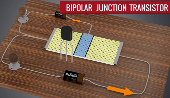
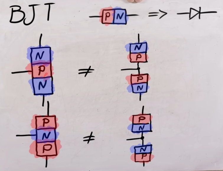
Bipolar transistors have many parameter symbols and their meanings. For example, B, C, and E represent the base, collector, and emitter respectively. Ib, Ic, and Ie represent the currents of the base, collector, and emitter, respectively, while Vcb, Vbe , Vce represents the voltage between the collector and the base, the emitter and the base, and the collector and the emitter.
Together, these parameter symbols define the operating characteristics of a bipolar transistor and are critical to understanding its performance and how it is used.
Bipolar transistor is a common electronic device. Its parameter symbols and their meanings are as follows:
Ic: collector current, refers to the DC current passing through the collector of the transistor under given conditions. The average value of collector DC or AC current.
Icbo: The reverse saturation current between the base and collector when the emitter is open circuit. The base is grounded, the emitter is open to ground, and the reverse cut-off current between the collector and the base under the specified VCB reverse voltage condition
Iceo: The reverse blocking current between the emitter and collector when the base is open circuit at a given temperature. The emitter is connected to ground and the base is open to ground. Under the specified reverse voltage VCE condition, the reverse cut-off current between the collector and emitter is reached.
Iebo: Reverse cutoff current between base and emitter when collector is open circuit at a given temperature. The base is grounded, the collector is open to ground, and under the specified reverse voltage VEB condition, the reverse cut-off current between the emitter and the base is reached.
IB: The average value of base DC current or AC current
IE: the average value of the emitter DC current or AC current
Icer: The series resistor R between the base and the emitter. When the voltage VCE between the collector and the emitter is a specified value, the reverse cut-off current between the collector and the emitter is
Ices: The emitter is grounded, the base is short-circuited to ground, and under the specified reverse voltage VCE condition, the reverse cut-off current between the collector and the emitter
Icex: The emitter is grounded, a specified bias voltage is applied between the base and the emitter, and under the specified reverse bias voltage VCE, the reverse cut-off current between the collector and the emitter
ICM: The maximum allowable current of the collector or the maximum average value of the AC current.
IBM: The maximum value of DC current that can continuously pass through the base within the range that the collector is allowed to dissipate power, or the maximum average value of AC current
ICMP: collector maximum allowable pulse current
ISB: secondary breakdown current
IAGC: forward automatic current control
Pc: collector dissipation power, which refers to the maximum power that the transistor can withstand during normal operation.
PCM: The maximum allowable power dissipation of the collector refers to the maximum power dissipation that the transistor can withstand under given conditions.
Pi: input power
Po: output power
Posc: oscillation power
Pn: noise power
Ptot: total power dissipated
VCB: Reverse breakdown voltage between collector and base.
VBE (Vb): forward voltage between base and emitter.
VCEO: Reverse breakdown voltage between collector and emitter.
VCES: Saturation voltage between collector and emitter.
β: Common base amplification factor, which refers to the ratio of the change of the output signal to the change of the input signal in the common base circuit.
α: Common emitter amplification factor, which refers to the ratio of the change amount of the output signal to the change amount of the input signal in the common emitter circuit.
fT: Characteristic frequency of the transistor, which refers to the highest operating frequency of the transistor.
fmax: The limit frequency of the transistor, which refers to the highest frequency at which the transistor can operate normally. The operating frequency when the triode power gain is equal to 1.
fmin: The lowest operating frequency of the transistor, which refers to the lowest frequency at which the transistor can operate normally.
fα: Common emitter cutoff frequency, which refers to the frequency point at which the amplification factor begins to decrease when the frequency of the input signal increases in the common emitter circuit.
fβ: The turning frequency of the frequency response of the common emitter signal source, which refers to the frequency point at which the amplification factor begins to decrease when the frequency of the input signal increases in the common emitter circuit.
fH: Common base cutoff frequency, which refers to the frequency point at which the amplification factor begins to decrease when the frequency of the input signal increases in the common base circuit.
fL: The turning frequency of the frequency response of the common base signal source, which refers to the frequency point at which the amplification factor begins to decrease when the frequency of the input signal increases in the common base circuit.
Vf: forward voltage drop, refers to the forward conduction voltage of the transistor.
Vr: Reverse voltage drop, refers to the reverse conduction voltage of the transistor.
VCBO: The base is grounded, the emitter is open to ground, and the maximum withstand voltage between the collector and the base under specified conditions
VEBO: The base is grounded, the collector is open to ground, and the maximum withstand voltage between the emitter and the base under specified conditions
VCEO: The emitter is grounded, the base is open to ground, and the maximum withstand voltage between the collector and emitter under specified conditions
VCER: The emitter is grounded, a resistor R is connected in series between the base and the emitter, and the maximum withstand voltage between the collector and the emitter under specified conditions
VCES: The emitter is grounded, the base is short-circuited to ground, and the maximum withstand voltage between the collector and emitter under specified conditions
VCEX: The emitter is grounded, a specified bias voltage is applied between the base and the emitter, and the maximum withstand voltage between the collector and the emitter under specified conditions
Vp: punch-through voltage.
VSB: Secondary breakdown voltage
VBB: Base (DC) power supply voltage (external circuit parameters)
Vcc: Collector (DC) power supply voltage (external circuit parameters)
VEE: Emitter (DC) power supply voltage (external circuit parameters)
VCE(sat): The emitter is grounded, and the saturation voltage drop between the collector and the emitter under Ic and IB conditions is specified.
VBE(sat): The emitter is grounded, and under specified Ic and IB conditions, the base-emitter saturation voltage drop (forward voltage drop)
VAGC: forward automatic gain control voltage
Vn(p-p): Peak equivalent noise voltage at the input end
V n: noise voltage
D: duty cycle
Bvceo: Reverse breakdown voltage, which refers to the maximum reverse voltage between the base and collector of a transistor during normal operation.
BVcbo: open emitter, breakdown voltage between collector and base
Bvbeo: Forward breakdown voltage refers to the maximum forward voltage between the base and emitter of a transistor during normal operation.
Bvces: saturation voltage drop, refers to the voltage drop between the base and emitter of the transistor when it is in saturation state. Base and emitter short circuit CE junction breakdown voltage.
BVebo: Open collector EB junction breakdown voltage.
BV cer: The base and emitter are connected in series with a resistor, CE junction breakdown voltage.
αF: forward current amplification factor, refers to the forward current amplification coefficient of the transistor.
αR: Reverse current amplification factor, which refers to the reverse current amplification coefficient of the transistor.
fmaxF: forward maximum operating frequency, refers to the upper limit of the forward operating frequency of the transistor.
fmaxR: reverse maximum operating frequency, which refers to the upper limit of the reverse operating frequency of the transistor.
fminF: forward minimum operating frequency, refers to the lower limit of the forward operating frequency of the transistor.
fminR: Reverse minimum operating frequency, which refers to the lower limit of the reverse operating voltage of the transistor.
Cj: Junction (interelectrode) capacitance, indicating the total capacitance of the germanium detection diode when a specified bias voltage is applied to both ends of the diode.
Cjv: bias junction capacitance
Cjo: zero bias junction capacitance
Cjo/Cjn: junction capacitance change
Cs: case capacitance or package capacitance
Ct: total capacitance
CTV: voltage temperature coefficient. The ratio of the relative change of the stable voltage to the absolute change of the ambient temperature under the test current
CTC: Capacitance temperature coefficient
Cvn: nominal capacitance
hFE: common emitter quiescent current amplification factor
hIE: common emitter static input impedance
hOE: common emitter static output conductance
h RE: Common emitter static voltage feedback coefficient
hie: total emission of very small signal short-circuit input impedance
hre: total emission of very small signal open circuit voltage feedback coefficient
hfe: total emission of very small signal short-circuit voltage amplification factor
hoe: total emission of very small signal open circuit output admittance
ESB: Second breakdown energy
rbb: base area extended resistance (base area intrinsic resistance)
rbbCc: base-collector time constant, which is the product of base extension resistance and collector junction capacitance
rie: input resistance when the emitter is grounded and the AC output is short-circuited
roe: The output resistance when the emitter is grounded and the AC input is short-circuited when measured under specified VCE, Ic or IE, and frequency conditions.
IF: Forward DC current (forward test current). The current passing through the inter-electrode of the germanium detection diode under the specified forward voltage VF; the maximum operating current (average value) allowed to pass continuously in the sinusoidal half-wave of the silicon rectifier and silicon stack under the specified conditions of use, and the silicon switch The maximum forward DC current allowed to pass through the diode under rated power; the current given when measuring the forward electrical parameters of the Zener diode.
IF (AV): forward average current
IFM (IM): Forward peak current (forward maximum current). The maximum forward pulse current allowed through the diode at rated power. LED limits.
What are the application scenarios of bipolar transistors?
The application scenarios of bipolar transistors mainly include the following aspects: In the fields of radio, television, communications, radar, computers, automatic control devices, electronic instruments, household appliances, etc., used for amplification, oscillation, switching and other functions. Traditional industries such as industry, communications, computers, consumer electronics, automotive electronics, aerospace, national defense and military industries, as well as emerging industries such as rail transit, new energy, smart grids, and new energy vehicles. Constitute amplifier circuits, or drive speakers, motors and other equipment, and are widely used in aerospace engineering, medical equipment, robots and other application products. As a key component of amplifiers in audio amplification, radio frequency amplification, video amplification and other fields.
What are the disadvantages of bipolar transistors?
Disadvantages of bipolar transistors include temperature sensitivity and bias, which can cause circuit instability. In addition, bipolar transistors may introduce noise that affects circuit performance. In high-speed switching circuits, the response speed of bipolar transistors is relatively slow and is not as stable as field effect transistors. In addition, bipolar transistors consume large amounts of power, require large drive currents, and are relatively large in size. Despite these shortcomings, bipolar transistors are still used in many fields because of their advantages such as fast response speed, high amplification, and low noise. Choosing the right transistor based on specific needs can improve the performance and stability of your circuit.
What is the meaning of collector current Ic, Ice, Ie?
The collector currents Ic, Ice, and Ie have the following meanings: Ic is the limit value, which refers to the collector current, and C represents the collector. The specific meaning of Ic is the maximum DC current of the collector. Iceo, ICES, and ICER are called transistor collector reverse current. Their names and meanings are as follows: When the emitter is open and a reverse voltage is applied between the collector and the base, the reverse current of the collector is usually called the reverse current. towards saturation current. Ie represents the current at the emission extreme. In addition, the transistor has three ports, E emitter, B base and C collector, and I represents the current, IE represents the current at the emitter terminal, IB represents the current at the base terminal, and IC represents the current at the collector terminal.
What are the applications of bipolar transistors?
Bipolar transistors have a wide range of applications, mainly including the following aspects: Communication field: Bipolar transistors are used for signal amplification, oscillation, switching, etc., and are widely used in radio, television, communications, radar and other fields. Industrial control field: As a key electronic device, bipolar transistors are used to realize amplification, switching, isolation and other functions of control circuits, and are widely used in industrial automation control systems. Consumer electronics: Bipolar transistors are used in audio amplification, video amplification, switching circuits, etc., and are key components in many electronic products. Automotive electronics: Bipolar transistors are used in automotive sensors, ignitions, lighting control and other circuits to function as signal amplification and switching. Aerospace field: Bipolar transistors have the characteristics of high reliability and long life, and are suitable for various electronic equipment in aerospace engineering. Medical device field: Bipolar transistors are used in sensors, amplifiers and other circuits in medical devices to perform signal processing and amplification. Robot field: Bipolar transistors are used in robot control systems and sensor circuits to achieve signal amplification and processing. Bipolar transistors have a wide range of applications, covering communications, industrial control, consumer electronics, automotive electronics, aerospace, medical equipment and robotics.
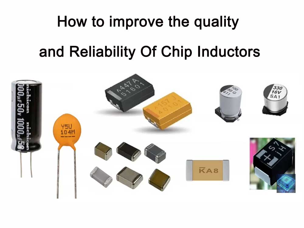
Chip inductors is one of the commonly used components in electronic equipment. It is mainly used to store energy and implement functions such as signal filtering, coupling and transmission.
Improving the quality and reliability of chip inductors is of great significance to ensure the performance and stability of electronic equipment. The following is a detailed introduction on how to improve the quality and reliability of chip inductors:
Selecting Inductor For Switching Power Supply – Not everyone knows this. – When using inductor consider also material, height, rotation …. Explained by Carmen Parisi.
Core material: Choosing a core material with high magnetic permeability and low loss can improve the performance of the chip inductor. Commonly used magnetic core materials include manganese-zinc ferrite, nickel-zinc ferrite and iron powder core.
Coil wire: The selection of coil wire is crucial to the quality and reliability of the inductor. Wires with high current carrying capacity, low DC resistance, high temperature resistance, corrosion resistance, etc. should be selected, such as copper wires, alloy wires, etc.
Packaging materials: Packaging materials should have the characteristics of high temperature resistance, good insulation performance, and high mechanical strength to ensure the stability and reliability of the inductor. Commonly used packaging materials include epoxy resin, ceramics, plastics, etc.
Chip inductor manufacturing process
Coil winding: During the coil winding process, the coils should be kept tight and even to avoid problems such as looseness and disconnection. At the same time, the number of turns and wire diameter of the coil should be controlled according to the design requirements to ensure the electrical performance of the inductor.
Magnetic core assembly: During the assembly process of the magnetic core, the position of the magnetic core should be ensured to avoid tilting, loosening, etc. At the same time, the assembly pressure should be controlled to avoid damage or deformation of the magnetic core.
Heat treatment process: The heat treatment process can improve the magnetic permeability of the magnetic core material and the mechanical strength of the coil wire. During the heat treatment process, the temperature and time should be controlled to avoid problems such as overheating and oxidation.
Surface treatment process: Surface treatment process can improve the corrosion resistance and aesthetics of the inductor. Commonly used surface treatment processes include gold plating, silver plating, plastic spraying, etc.
Optimization of chip inductor structure
Optimize the coil structure: By optimizing the coil structure, the DC resistance of the coil can be reduced and the heating performance and reliability of the inductor can be improved. For example, methods such as winding multiple strands in parallel and increasing the cross-sectional area of the coil are used.
Optimize the magnetic core structure: By optimizing the magnetic core structure, the magnetic permeability of the magnetic core can be increased, the magnetic loss and heat loss can be reduced, thereby improving the performance and reliability of the inductor. For example, methods such as using high magnetic permeability core materials and reducing the cross-sectional area of the core are used.
Optimize the packaging structure: By optimizing the packaging structure, the mechanical strength and stability of the inductor can be improved, thereby improving its reliability. For example, methods such as using reinforcing ribs and increasing package thickness are used.
Chip inductor quality control
Strictly control material quality: Conduct quality inspections and tests on purchased materials to ensure that the quality of the materials meets requirements. At the same time, material quality files are established to track and control the quality of materials.
Strengthen manufacturing process control: Develop strict manufacturing process and quality control standards, and monitor and record the entire manufacturing process. Timely discover and solve problems that arise during the manufacturing process to ensure product quality and reliability.
Finished product inspection and testing: Conduct comprehensive inspection and testing of finished products, including electrical performance testing, appearance inspection, environmental adaptability testing, etc. Ensure that product performance and quality meet requirements, and trace and handle unqualified products.
Establish a quality assurance system: Establish a complete quality assurance system, including quality planning, quality control, quality assurance, etc. Through continuous improvement and improvement of the effectiveness of the quality assurance system, we continuously improve the quality and reliability of our products.
To sum up, improving the quality and reliability of chip inductors requires starting from aspects such as material selection, manufacturing process, structural optimization and quality control.
Through reasonable material selection and manufacturing processes, optimizing product structure, and strengthening the construction of quality control and quality assurance systems, the quality and reliability of chip inductors can be effectively improved, providing a strong guarantee for the efficient and stable operation of electronic equipment.
Methods to improve the service life of chip inductors
How to improve the service life of chip inductors? If you want to improve the service life of chip inductors, you can proceed from the following aspects:
Choose high-quality chip inductors: Choose inductor products produced by regular manufacturers to ensure their quality and reliability. Regular large manufacturers are more stringent in raw material procurement, production process control, quality inspection, etc., and can ensure the performance and quality of chip inductors. Chip inductors produced by regular manufacturers are more reliable in quality and have longer service life. When choosing chip inductors, you should give priority to brands and manufacturers with quality assurance.
Optimize the structure of the chip inductor: According to actual needs and application scenarios, optimize the coil, magnetic core and other structures of the chip inductor to improve its stability and reliability. For example, optimizing the winding method of the coil and increasing the cross-sectional area of the coil can improve the heating performance and reliability of the inductor. Core material and structure have an important impact on the performance and service life of chip inductors. Choosing magnetic core materials with high magnetic permeability and low magnetic loss, as well as optimizing the structure and size of the magnetic core, can improve the stability and reliability of the chip inductor and extend its service life.
Select appropriate coil wire materials: The selection of coil wire materials has a crucial impact on the service life of the chip inductor.
Choosing high-temperature-resistant, low-impedance coil wire can improve the current-carrying capacity and reliability of the chip inductor, thereby extending its service life.
Choosing packaging materials with good temperature resistance, moisture resistance, corrosion resistance and other properties can improve the protection effect and service life of the chip inductor.
Choose high-temperature resistant, low-impedance coil wires: The selection of coil wires has a crucial impact on the service life of the chip inductor. Choosing high temperature resistant, low impedance coil wire can improve the current carrying capacity and reliability of the chip inductor.
Avoid overload use: When using chip inductors, overload use should be avoided to avoid problems such as coil overheating and core saturation, which will affect the service life of the chip inductor.
Pay attention to the working environment temperature: The working environment temperature of the chip inductor also affects its service life. The working environment temperature of the chip inductor should be reduced as much as possible and long-term high-temperature operation should be avoided to increase its service life.
Correct installation and use: When installing and using chip inductors, the correct direction and position should be followed to avoid the impact of mechanical stress, vibration and other factors on the chip inductor to ensure its service life.
Regular maintenance and inspection: For chip inductors that have been used for a long time, regular maintenance and inspection should be carried out to detect and solve potential problems in time to extend their service life.
Improving the service life of chip inductors requires ensuring quality, optimizing structure, selecting appropriate coil wires, avoiding overload use, paying attention to the working environment temperature, correct installation and use, and regular maintenance and inspections.
To sum up, improving the service life of chip inductors requires selecting high-quality chip inductors, suitable coil wires, optimizing core materials and structures, avoiding overload use, paying attention to the working environment temperature, correct installation and use, and regular maintenance.
Start with inspection and selection of appropriate packaging materials. At the same time, in practical applications, you should also pay attention to comply with the usage specifications and precautions to ensure that the service life of the chip inductor is fully guaranteed.
How should the coil wires of chip inductors be selected and optimized
When selecting and optimizing coil wires for chip inductors, the following aspects need to be considered:
DC resistance: The DC resistance of the coil wire will affect the heating performance and power consumption of the inductor. Choosing coil wire with lower DC resistance can improve the inductor’s heating performance and reliability.
Current carrying capacity: The current carrying capacity of the coil wire is one of the key factors in selecting the wire. When selecting coil wires, wires with sufficient current carrying capacity should be selected based on the operating current and peak current requirements of the inductor.
Mechanical strength: Coil wire needs to have a certain mechanical strength to withstand the mechanical stress during manufacturing and assembly. Choosing coil wire with higher mechanical strength can improve the stability and reliability of the inductor.
High temperature resistance: The high temperature resistance of the coil wire is one of the key factors affecting the reliability of the inductor. Choosing coil wire materials with higher high temperature resistance can improve the service life and reliability of the inductor.
Environmental protection requirements: In modern electronic products, environmental protection requirements are getting higher and higher. Choosing coil wires that meet environmental protection requirements, such as lead-free, low-smoke halogen-free and other environmentally friendly wires, can improve the environmental performance and market competitiveness of the inductor.
In order to optimize the selection of coil wire materials, the following aspects can be considered:
Select appropriate coil wire specifications and models based on actual needs and application scenarios.
On the premise of meeting performance requirements, give priority to coil wires with lower cost and environmental protection requirements.
During the manufacturing process, pay attention to the quality control of the coil wire and the optimization of the processing technology to ensure the quality and reliability of the coil wire.
During use, pay attention to the monitoring and adjustment of the working environment temperature and current carrying capacity of the coil wire to avoid the impact of overload and high temperature on the coil wire.
To sum up, selecting and optimizing coil wires for chip inductors requires comprehensive consideration of DC resistance, current carrying capacity, mechanical strength, high temperature resistance, environmental protection requirements and other factors.
At the same time, during the manufacturing and use processes, quality control and process optimization are strengthened to ensure the quality and reliability of coil wires, thereby improving the service life and stability of chip inductors.
So if the chip inductor has been damaged, is it still possible to repair it
Whether the chip inductor can be repaired after damage depends on the degree of damage and the specific cause. Here are some possible fixes:
Replace the inductor: If the inductor is completely damaged or cannot be repaired, the best way is to replace it with a new inductor. Please note that if you know the model number of the inductor, you can buy it online and replace it yourself. If you are not sure about the model, it is best to consult a professional technician and ask them to replace it.
Welding repair: If the coil of the inductor is disconnected or has poor contact, you can consider using welding to repair it. Please note that proper solder and soldering temperature should be used when soldering to avoid damage to other components.
Winding the coil: If the coil of the inductor is damaged, consider re-winding the coil. Please note that proper wire diameter and number of turns should be used during winding to restore the electrical properties of the inductor.
Secure the core: If the inductor’s core becomes loose or falls off, consider using appropriate glue or fixtures to re-fix the core in the correct position.
It should be noted that for some complex chip inductors, the repair process may require professional techniques and tools.
Therefore, before carrying out repairs, it is best to consult professional technicians or relevant experts to understand the feasibility of repairs and choose appropriate repair methods.
At the same time, when repairing and maintaining any electronic equipment, you must pay attention to safety to avoid damage to the equipment and people.
If my chip inductor is overloaded, how should I check and repair it
If the chip inductor is overloaded, you first need to check whether the appearance of the inductor is burnt, discolored, cracked, etc., and whether there is any abnormal sound or smell. These signs may indicate that the inductor is damaged.
If the visual inspection reveals no problems, you can use a multimeter to check the resistance value of the inductor. The resistance value of a normal inductor should be close to zero. If the resistance value is very large or infinite, it may indicate that the inductor has been damaged.
If it is determined that the inductor is damaged, the cause of the damage needs to be found and corresponding repair measures must be taken. Common repair methods include replacing inductors, welding repairs, winding coils, and fixing cores. The specific repair method needs to be determined based on the degree of damage and the cause of the damage.
When repairing chip inductors, you need to pay attention to safety issues. When replacing inductors or soldering, problems such as short circuits or overheating need to be avoided to avoid damage to the circuit board and other components. At the same time, appropriate tools and materials, such as suitable soldering stations, soldering tin, solder paste, etc., need to be used to ensure the quality and reliability of the repair.
In addition, in order to prevent overloading of chip inductors, some preventive measures can be taken, such as controlling the stability of the power supply voltage, avoiding overloading of the power supply line, and selecting appropriate inductors and components. These measures can effectively reduce the possibility of inductor overload and improve the stability and reliability of the circuit.
How should the withstand voltage and current values of chip inductors be selected and optimized
When selecting and optimizing the withstand voltage and current values of chip inductors, the following aspects need to be considered:
Circuit requirements: Determine the required withstand voltage and current values based on the operating voltage and current of the circuit. If the working voltage of the circuit is high, you need to choose an inductor with a higher withstand voltage value; if the working current of the circuit is large, you need to choose an inductor with a larger current value.
Magnetic core material: Parameters such as magnetic permeability and saturation flux density of the magnetic core material will affect the performance of the inductor. Choosing a core material with high magnetic permeability and saturation flux density can improve the withstand voltage and current values of the inductor.
Coil wire: Parameters such as the cross-sectional area and resistance value of the coil wire will also affect the performance of the inductor. Choosing a coil wire with a larger cross-sectional area and smaller resistance value can increase the current value of the inductor.
Package size: Package size will affect the heat dissipation performance and mechanical strength of the inductor. When selecting the package size, heat dissipation needs and mechanical strength requirements need to be considered to ensure the performance and reliability of the inductor.
Working environment temperature: The working environment temperature of the inductor will affect its performance and reliability. When selecting an inductor, you need to consider the influence of the working environment temperature and select an inductor with corresponding temperature resistance.
In order to optimize the withstand voltage value and current value of the chip inductor, the following aspects can be considered:
Optimize the structure and size of the magnetic core: By optimizing the structure and size of the magnetic core, the withstand voltage and current values of the inductor can be further improved. For example, increasing the cross-sectional area of the magnetic core and reducing the number of turns of the coil can increase the current value.
Optimize the coil design: Optimizing the coil design can improve the performance and reliability of the inductor. For example, adopting appropriate winding methods and number of turns, selecting appropriate coil wire materials and other measures can improve the current value and voltage resistance value of the inductor.
Strengthen the heat dissipation design: Strengthening the heat dissipation design can improve the heat dissipation performance and stability of the inductor. For example, measures such as adding heat sinks and improving heat dissipation channels can improve the withstand voltage and current values of the inductor.
Use high-quality raw materials: Using high-quality raw materials can improve the performance and reliability of the inductor. For example, choosing core materials with high magnetic permeability and saturation magnetic flux density, selecting coil wires with low resistance values, and other measures can improve the withstand voltage and current values of the inductor.
To sum up, selecting and optimizing the voltage and current values of chip inductors requires comprehensive consideration of circuit requirements, core materials, coil wires, package size, working environment temperature, etc.
At the same time, during the manufacturing and use processes, quality control and process optimization are strengthened to ensure the quality and reliability of chip inductors.
What are the main factors of the temperature resistance of the patch
The temperature resistance of the patch inductor mainly depends on the following factors:
The quality of raw materials: High -quality raw materials have better stability and reliability, and can effectively extend the life of the inductance. For example, a magnetic core material with high magnetic guidance, low magnetic damage, and coil wires with high temperature resistance and low impedance.
Structural design: By optimizing the structural design of the inductance, the heat loss of the inductance can effectively reduce the heat loss of the inductance in high temperature, thereby improving the temperature resistance. For example, measures such as optimizing coil winding and increasing the cross -area of the coil can improve the thermal performance and reliability of the inductance.
Heating design: In order to prevent inductance from overheating in high temperature environments, the heat dissipation design of inductance needs to be strengthened. For example, increased heat dissipation pieces and selection of materials with good thermal conductivity can improve the heat dissipation performance and temperature resistance of inductance.
Production process: In the process of inductance, the production process must be strictly controlled to ensure the quality of the inductance, and the temperature resistance of temperature resistance is reduced due to the problem of production technology. For example, strictly control the winding process of the coil and the assembly process of magnetic cores.
In summary, the temperature resistance of improving the inductance of the patch needs to be started from choosing high -quality raw materials, optimizing structural design, strengthening heat dissipation design, and strict control of production technology.
At the same time, in practical applications, we should also pay attention to compliance with the use specifications and precautions to ensure that the temperature resistance of the patch is fully guaranteed.