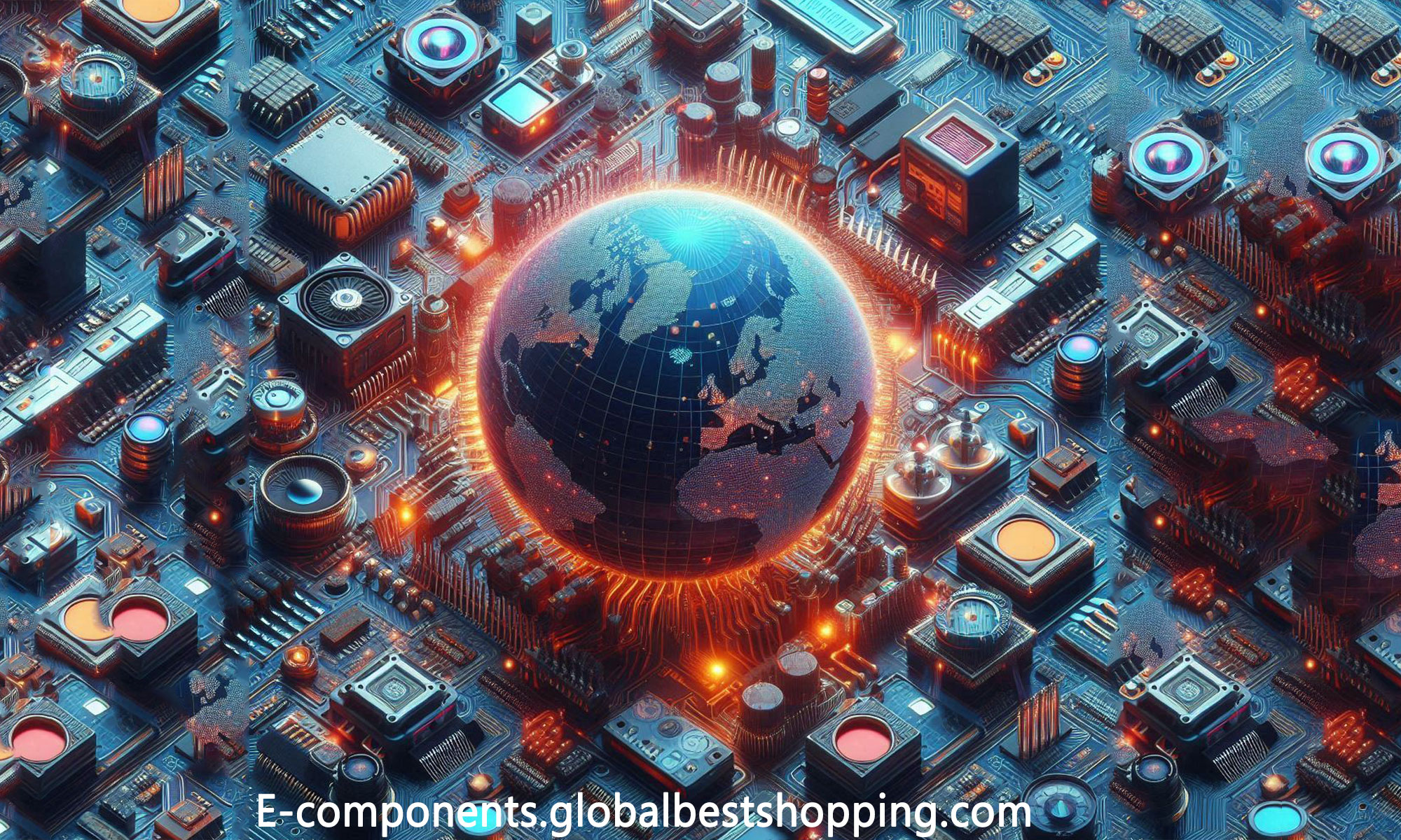
In nanotechnology, nanoelectronic components refer to electronic components manufactured using nanotechnology, and their dimensions are usually at the nanometer level (ie, between 1 nanometer and 100 nanometers).
Due to their extremely small size, nanoelectronic components have many unique properties and advantages, and therefore have broad application prospects in the field of electronic technology in the future.
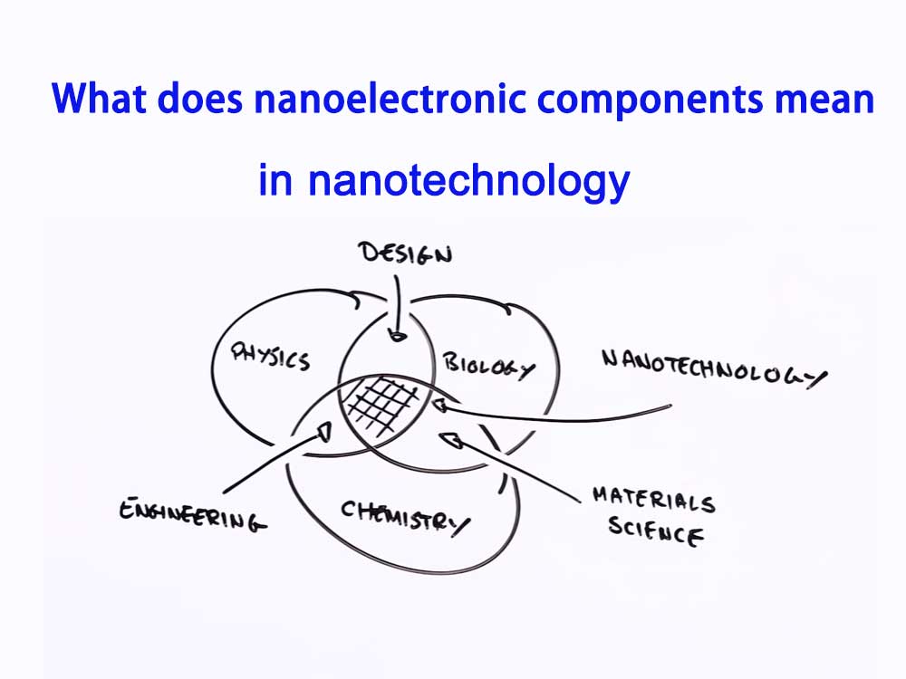
Overview of Nanoelectronic Components
The core technology of nanoelectronic components is nanotechnology, which involves knowledge from multiple disciplines such as physics, chemistry, and materials science.
At the nanometer level, the properties of matter undergo significant changes, which provides new possibilities for the design and manufacture of electronic components.
Compared with traditional electronic components, nanoelectronic components have higher performance, lower power consumption and smaller size, and are therefore considered to be one of the key technologies for the next generation of electronic technology.
At present, people have used nanoelectronic materials and nanolithography technology to develop many nanoelectronic devices, such as electron resonance tunneling devices, resonant diodes, tripole resonance tunneling transistors, single electron transistors, metal-based, semiconductors, nanoparticles, single electron transistors, etc.
Electronic electrometer, single electron memory, single electron logic circuit, metal-based single electron transistor memory, semiconductor memory, memory made of silicon nanocrystals, nano floating gate memory, nano silicon microcrystalline thin film devices and polymer electronic devices, etc.
Nanoelectronics technology refers to related technologies that construct nano and quantum devices within the nanometer size range and integrate nano circuits to realize information calculation, transmission and processing of quantum computers and quantum communication systems. Among them, nanoelectronics devices are the current development of nanoelectronics technology. The key and core. Nowadays, nanoelectronics technology is in a period of vigorous development.
Its ultimate goal is to break through the traditional physical size and technical limits based on the latest physical theory and the most advanced process methods, and develop the potential information and structural potential of matter. According to new concepts, Design and manufacture nanodevices and construct electronic systems to achieve a revolutionary leap in the ability of electronic systems to store and process information.
Definition of Nanoelectronic Devices
Nanoelectronic devices refer to electronic devices with nanoscale scale and specific functions designed and prepared using nanoscale processing and preparation technologies, such as photolithography, epitaxy, microfabrication, self-assembly growth and molecular synthesis technology.
Background introduction to nanoelectronic devices
Nanotechnology is a high-tech discipline that studies and applies the motion patterns and characteristics of electrons, atoms and molecules within a 0.1-100um scale space. Its goal is to use single atoms and molecules to create products with specific functions.
Domestic and foreign scientific and technological circles have generally believed that nanotechnology has become the most dynamic research object in today’s research field and is very important to future economic and social development. Nanotechnology is promoting huge changes in human society. It will not only promote a revolution in human understanding, but also trigger a new industrial revolution.
Nanotechnology is a new field of science and technology that emerged in the late 20th century. It is a new high-tech subject group, including nanoelectronics, nanophotonics, nanophotonics, nanophysics, nanooptics, nanomaterials, and nanomachinery. science, nanobiology, nanometrics, nanotechnology, nanomedicine, nanomicroscopy, nanoinformation technology, nanoenvironmental engineering and nanomanufacturing, etc. It is an emerging technology that integrates basic research and application exploration.
Nanoelectronics is the detection, identification and control of the movement patterns of single quantum or quantum waves within 0.1~100nm nanostructures (quantum dots), and the study of artificial assembly and self-assembly technology of individual atoms and molecules. Research within quantum dots, The characteristics and functions exhibited by a single quantum or quantum wave are devices, circuits and systems used for the generation, transmission and exchange of information and their applications in information science and technology, nanobiology, nanometry, nanomicroscopy, nanomechanics, etc. An applied discipline, also known as quantum functional electronics.
Nanoelectronics is an important part of nanotechnology, an inevitable result of the development of traditional microelectronics, and the main driving force for the development of nanotechnology. Nanoelectronics is based on traditional solid-state electronics, using the latest physical theory and the most advanced process methods to construct electronic devices and systems according to new concepts. Nanoelectronics has the ability to develop the potential information and structure of matter at a deeper level, increasing the ability to store and process information per unit volume of matter by more than a million times, achieving a revolutionary breakthrough in information collection and processing capabilities.
Nanoelectronics is combined with optoelectronics, biology, mechanics and other disciplines to produce nanoelectronics/optoelectronic devices, molecular devices, nanoelectronic mechanical systems, nanooptoelectronic mechanical systems, micro-robots, etc., which will have an impact on human production and lifestyle. Producing a transformative impact, nanoelectronics/optoelectronics will become a key science and technology in the information age of the 21st century.
According to Moore’s Law, in the next 10 years or so, continuing to improve the storage density and computing power of computers will face severe challenges. These challenges include both theoretical physical limitations and technical process limitations. Its main manifestation is that when the size of the electronic device is on the order of microns, the electrons in it are mainly particulate. But when the size of the device is as small as nanometers, the electrons are mainly wave-like. The volatility of electrons is a quantum effect.
At this time, electronic devices will work under a completely new principle; any multi-body system has thermal statistical fluctuations. When the size of the device is reduced to the nanometer level, this thermal fluctuation will It will limit the consistency of device performance, causing the integrated chip to fail to work properly.
However, the emergence of nanoelectronics technology, nanoelectronic devices and nanoelectronics has provided new ways and opportunities for the development of microelectronics technology.
On the one hand, this can be attributed to the continuous development of microelectronics and nanotechnology; on the other hand, it can be attributed to the powerful contributions provided by microelectronics and quantum physics to the preparation, characteristics, mechanism and characterization of nanoelectronic devices over more than half a century. support.
Classification of Nanoelectronic Devices
Based on current development and predictions for the future, if the main nanoelectronic devices are further classified, nanoCMOS devices mainly include: silicon-on-insulation MOSFET, silicon-germanium heterogeneous MOSFET, low-temperature MOSFET, bipolar MOSFE T, and intrinsic silicon trench Tunnel type MOSFET, etc.; quantum effect devices include: quantum interference devices, quantum dot devices and resonant tunnel devices, and resonant tunnel devices include: lateral resonant tunnel devices, resonant tunnel transistors, resonant tunnel field effect transistors (RTEET), dual Polar quantum resonant tunnel transistors, resonant tunnel hot electron transistors, longitudinal resonant tunnel devices and tunnel barrier modulation transistors, etc.; single electron devices mainly include: single electron boxes, capacitor coupled and resistor coupled single electron transistors, single electron neural network transistors , single-electron junction array, single-electron pump, single-electron trap and single-electron revolving door, etc.; single-atom devices and single-molecule devices include: single-electron switches, single-atom point contact devices, single-molecule switches, molecular wires, quantum effect molecules Electronic devices, electrochemical molecular electronic devices, etc.
Nanosensors include
Quantum tunnel sensors and nano-biosensors; nano-integrated circuits, nano-electronic integrated circuits and nano-optoelectronic integrated circuits. Nano-memory includes: ultra-high-capacity nano-memory, ultra-high-density data memory, tunnel-type static random access memory, single-electron silicon-based MOS memory , single-electron memory, single-electron quantum memory; nano-CMOS hybrid circuits include: nano-CMOS circuits and 1-V compound semiconductor resonance tunneling effect circuits, nano-CMOS circuits and single-electron nano-switch circuits, nano-CMOS circuits and superconducting single magnetic flux quantum circuits Circuits, the marriage of nano-CMOS circuits and carbon nanotube circuits, nano-CMOS circuits and artificial atomic circuits and artificial molecular circuits, nano-CMOS circuits and DNA circuits, nano-CMOS circuits and nano-metal-based spin circuits, and other mainstream circuits, provide a basis for nanoelectronics Created a new development. Nano 1`V compound semiconductor devices and circuits refer to resonant tunnel diodes and resonant tunnel transistors and circuits. It has strong potential in the fields of high speed, high frequency and optoelectronics.
Scientists predict that in the 21st century, nanoelectronic devices, nano optoelectronic devices, nano Integrated circuits and nano-optoelectronic integrated circuits are the most promising.
Sensors manufactured using nanotechnology have higher sensitivity and smaller size and can be used in medical, environmental protection, military and other fields. For example, biosensors based on single-walled carbon nanotubes can be used to detect biomolecules and cells.
Nanosingle electron devices
Many nanoelectronic devices have been developed using nanoelectronics using nanoelectronic materials and nanolithography technology, such as: electron resonance tunneling devices, electron resonance tunneling devices, resonant diodes (RTD), and three-terminal resonant tunneling transistors (RTT). ), single electron transistor (SET), single island single electron transistor (SET), metal-based SET, semiconductor SET, nanoparticle SET, multi-island SET, single electron electrometer, single electron memory (SEM), single electron logic circuit, Single electron cMOS circuit, metal-based single electron transistor (sET) memory, semiconductor SET memory, memory made of silicon nanocrystals, nano floating gate memory, single electron digital integrated circuit, single electron transistor (sET) logic integrated circuit , nano silicon microcrystalline thin film devices (such as resonant tunneling diodes (RTD)) and polymer electronic devices, etc.
nanotransistor
This is the most basic type of nanoelectronic components, with dimensions ranging from a few to tens of nanometers. Compared with traditional transistors, nanotransistors have faster switching speeds and lower power consumption, so they have broad application prospects in high-speed, low-power integrated circuits.
Electronic wave devices
Electron wave interference devices, short-line waveguide interference devices, MachZender interferometers (electrostatic interference devices), directional coupling devices, diffraction devices, quantum wire channel field effect transistors (FETs), planar superlattice FETs, electron velocity modulation FET resonant tunnels Wearing devices, etc.
The electrons in quantum wave devices are in a phase-coherent structure, and their behavior is mainly wavelike. Such devices include quantum wire transistors, quantum interference devices, resonant tunneling diode transistors, etc.
Nano solar cells
Nanostructures are used to improve the light absorption efficiency and photoelectric conversion efficiency of solar cells, with higher energy conversion efficiency and smaller size. For example, solar cells based on titanium dioxide nanorods have excellent performance.
nanomemory
Memories manufactured based on nanotechnology have higher storage density and faster read and write speeds. For example, carbon nanotube random access memory is a type of memory based on carbon nanotubes that has a storage density several orders of magnitude higher than traditional flash memory.
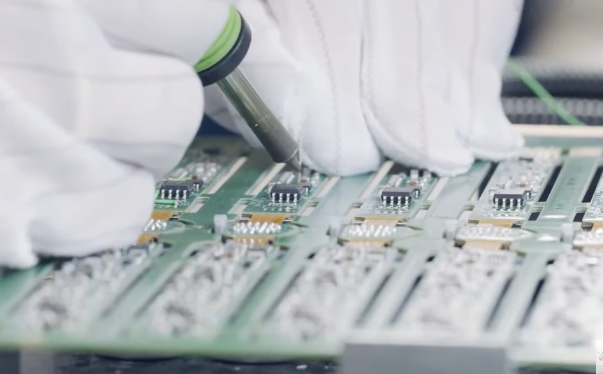
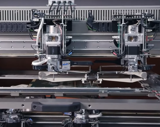
Preparation Technology of Nanoelectronic Devices
To prepare nanoelectronic devices and realize their integrated circuits, there are two possible ways. One is to further extend existing electronic devices and integrated circuits toward miniaturization, and research and develop processing technology with smaller line widths to process smaller electronic devices, which is the so-called “top-to-bottom” approach.
Another way is to use advanced nanotechnology and the quantum effects of nanostructures to directly form new quantum devices and quantum structure systems, which is the so-called “bottom-up” approach.
The “top-to-bottom” preparation method of nanoelectronic devices mainly refers to technologies such as optical lithography, electron beam lithography, and ion beam lithography.
“Bottom-up” preparation methods include metal-organic chemical vapor deposition, molecular beam epitaxy, atomic layer epitaxy, chemical beam epitaxy and other epitaxy technologies, scanning probe microscopy technology, molecular self-assembly synthesis technology and special ultra-fine processing technology wait.
Lithography
Optical lithography, electron beam lithography and ion beam lithography technology are collectively referred to as three-beam lithography technology.
Processing technology that transfers designed device pattern structures to semiconductor substrates. At present, as the line width of lithography technology continues to decrease, optical lithography, electron beam lithography and ion beam lithography have shown good applications in the processing fields of nano devices, nano integrated circuits, nano hybrid circuits and so on. prospects, and has begun to be applied in the processing of some nanoelectronic devices.
Optical lithography technology
Optical lithography is a technology that uses an optical system to “engrav” the large-scale integrated circuit device structure pattern on the mask onto a silicon wafer coated with photoresist using a projection method. It is now the mainstream technology for industrial semiconductor processing. In this technique, methacrylate polymers are typically used as the resist coating and a mixture of methyl isobutyl ketone and isopropyl alcohol is used as the developer.
At present, the most attracting hot spot in the international microelectronics field is the new generation of photolithography technology. Limiting the minimum line width that can be obtained by lithography is directly related to the resolution of the lithography system, and reducing the wavelength of the light source is the most effective way to improve the resolution of lithography.
Now, the light source wavelength of commercial lithography machines has entered the deep ultraviolet band from the past mercury lamp source ultraviolet band. In addition, using the interference characteristics of light and electromagnetic theory combined with in-depth analysis of exposure imaging in lithography practice, Optimizing process parameters using various wavefront technologies is also an important means to improve lithography resolution.
electron beam lithography
Electron beam lithography is a photolithography technology that uses high-energy electron beams to expose photoresist to obtain structural patterns.
Recently, the angle-limited scattered projection electron beam lithography technology developed by Lucent in the United States is attracting attention. This technology reduces the projection of the mask pattern like optical lithography, and uses special filtering technology to remove scattered electrons generated by the mask absorber.
This improves output efficiency while ensuring resolution. It should be pointed out that no matter what technology is used in lithography in the future, it will be an indispensable infrastructure for integrated circuit research and production.
Ion beam lithography
Ion beam lithography is a photolithography technology that uses ions formed after ionization of liquid atoms or gaseous atoms to expose photoresist after being accelerated by an electromagnetic field and focused or collimated by an electromagnetic lens.
Its principle is similar to that of electron beam lithography, but the de Broglie wavelength is shorter, and has the advantages of no proximity effect, small exposure field, etc. Ion beam lithography mainly includes focused ion beam lithography, ion projection lithography, etc. epitaxial technology
Metal-organic chemical vapor deposition, molecular beam epitaxy, atomic layer epitaxy and chemical beam epitaxy technology are collectively referred to as epitaxial technology. It is a nano-manufacturing technology that grows nano-films on a substrate. It can be used for silicon-based semiconductor materials for nano-integrated circuits, nanometer Semiconductor structures: Device processing and preparation.
The beam intensity is proportionally sprayed onto the heated substrate surface, and ultimately interacts with the surface for epitaxial growth of single crystal films. The baffle in front of each blast furnace is used to change the composition and doping of the epitaxial film.
According to the set program, the baffle is opened and closed, the furnace temperature is changed, and the growth time is controlled.
Compounds with different thicknesses or ternary and quaternary solid solutions with different composition ratios and their heterojunctions can be grown, thereby preparing various ultra-thin products. Microstructured materials.
Research progress of nanoelectronic components
In recent years, with the development of materials science, physics, chemistry and other disciplines, the research on nanoelectronic components has made significant progress.
In the laboratory, people have successfully prepared various types of nanoelectronic components and conducted in-depth research on their properties.
At the same time, with the continuous advancement of manufacturing processes, the manufacturing costs of nanoelectronic components are gradually decreasing, making their commercial applications possible.
Challenges and Prospects of Nanoelectronic Components
Although nanoelectronic components have many advantages and broad application prospects, their research and application also face many challenges.
For example, how to control the size and performance of nanoelectronic components during the manufacturing process, how to improve their stability and reliability, how to achieve mass production and commercial applications, etc.
In addition, since nanoelectronic components involve knowledge in multiple subject areas, interdisciplinary cooperation and communication are required to solve the problems.
In the future, with the continuous advancement of technology and increasing application requirements, the research and application of nanoelectronic components will usher in broader development prospects. People expect nanoelectronic components to bring smaller size, higher performance, lower power consumption and lower cost to future electronic products.
At the same time, with the improvement of environmental awareness, the concepts of green, renewable and sustainable development will also be introduced into the research and application of nanoelectronic components.
For example, using renewable energy to manufacture nanoelectronic components and realizing environmentally friendly treatment of discarded nanoelectronic components.
In general, nanoelectronic components are one of the important development directions in the field of electronic technology in the future. Although there are still many challenges and problems that need to be solved, with the continuous advancement of science and technology and the continuous improvement of application requirements, it is believed that these problems will also be effectively solved.
In the future, we look forward to more innovations and breakthroughs in the field of nanoelectronic components to contribute to the sustainable development of human society.
Recommendations for future development of nanoelectronic devices
Attention must be paid to and vigorously carried out research on nano-devices, especially nano-electronic devices and nano-optoelectronic devices.
Academician Bai Chunli once pointed out that “the level of development and application of nano-devices is an important indicator of whether we have entered the nano-era”, and pointed out that “China must pay attention to the research work on the development of nano-devices and nano-scale detection and characterization.”
According to the current status of my country’s nanotechnology development, we must vigorously advocate the research, development and application of nanodevices, especially nanoelectronic devices and nanooptoelectronic devices.
Because the research on nanoelectronic devices and nano-optoelectronic devices is the fulcrum of the two major technologies of nanotechnology and information (electronic information and optoelectronic information) technology, it plays a vital role in the economy and the entire science and technology.
In terms of research and development of nanoelectronic devices and nano-optoelectronic devices, in addition to strengthening research on nano-electronic devices such as RTDs and SEDs, as well as nano-optoelectronic devices such as nano-lasers, nano-infrared photodetectors, and nano-optoelectronic integrated circuits, we must also vigorously and promptly Carry out research on molecular electronic devices. Internationally, the United States and Japan attach great importance to the research of molecular electronics.
The World’s Top Ten Scientific and Technological Advances reported the news that the United States had developed a molecular transistor. That is, Bell Labs used a single organic molecule to create the world’s smallest transistor. This is a molecular electronic device.
This type of chemical organic synthesis method can significantly reduce the cost of manufacturing electronic devices compared to using EB, MSE and other technologies to manufacture RTDs and SEDs, and is suitable for mass production. Chemists, electronics scientists, and optoelectronists should be called upon to work closely together to jointly carry out research on molecular electronic devices.