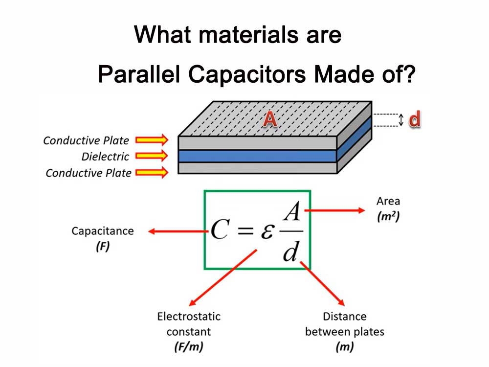
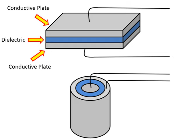
Parallel capacitors are usually made of aluminum metal film, polypropylene film, epoxy resin and other materials.
Below is a detailed introduction to these materials:
aluminum metal film
Aluminum metal film is one of the most common capacitor electrode materials and has good electrical conductivity and corrosion resistance. During the capacitor manufacturing process, an aluminum metal film is usually deposited on a polypropylene film by evaporation or sputtering to form a metal film.
The thickness of aluminum metal film is generally between 100-300 nanometers. It has good self-healing ability and high dielectric constant, making the capacitor have high capacitance.
Electrode material is another core component of the capacitor, which determines the conductive properties of the capacitor.
Commonly used electrode materials include aluminum foil, tantalum, silver, gold, etc. Aluminum foil is the most commonly used electrode material because of its good conductivity and cost-effectiveness. Tantalum and silver also conduct electricity well, but they cost more. Gold conducts electricity very well, but it’s also very expensive.
What’s inside the capacitor? Let’s Find Out. – Capacitor production experts explain the internal structure principles of capacitors
For electrode materials, commonly used electrode materials include:
Aluminum
Aluminum has good electrical conductivity and corrosion resistance, and is a commonly used material for making capacitors.
Silver
Silver has good electrical conductivity and high temperature resistance, and is a commonly used material for making high-frequency capacitors.
Gold
Gold has good electrical conductivity and oxidation resistance, and is another commonly used material for making high-frequency capacitors.
polypropylene film
Polypropylene film is another common capacitor insulating material with good electrical properties, mechanical properties and chemical stability.
In the manufacturing process of capacitors, polypropylene films are usually made by biaxial stretching and have the characteristics of high crystallinity, high mechanical strength, and excellent electrical properties. The thickness of polypropylene film is generally between 2-10 microns and has a low dielectric constant, allowing the capacitor to have low dielectric loss and heat loss.
Epoxy resin
Epoxy resin is a common organic polymer material with good insulation properties, adhesion properties and temperature resistance.
In the capacitor manufacturing process, epoxy resin is often used as an impregnating agent and sealing material, which can effectively protect the internal components of the capacitor and increase the mechanical strength of the capacitor.
At the same time, epoxy resin can also improve the insulation performance and temperature resistance of capacitors, allowing capacitors to operate at higher temperatures and voltages.
In addition to the above main materials, parallel capacitors also require other auxiliary materials, such as pins, insulators, casings, etc. The selection and use of these auxiliary materials also affects the performance and reliability of the capacitor.
Dielectric material
The dielectric material is the core component of the capacitor, which determines the capacitance of the capacitor.
Commonly used media materials include:
Ceramic materials
Ceramic materials have good electrical insulation properties and stability and are commonly used materials for making capacitors.
Plastic material
Plastic material has good electrical insulation properties and corrosion resistance, and is another commonly used material for making capacitors. Commonly used plastic materials include polyethylene, polypropylene, polytetrafluoroethylene, etc.
Paper capacitor
Paper capacitor has good electrical insulation properties and high voltage resistance, and is a commonly used material for making high-voltage capacitors.
The material selection of parallel capacitors needs to be based on the specific application of the capacitor. For example, for capacitors that require high capacitance and stability, ceramic or plastic dielectrics can be used, and electrode materials such as aluminum or silver can be used.
For capacitors that require high-frequency characteristics, paper capacitors can be selected and electrode materials such as gold or silver can be used.
The material selection and use of a shunt capacitor has a significant impact on its performance and reliability. In practical applications, appropriate materials and manufacturing processes need to be selected according to specific requirements to ensure optimal performance and reliability of shunt capacitors.
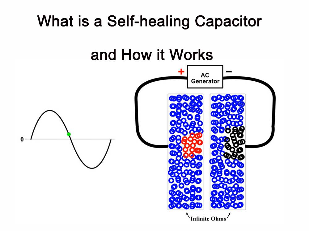
The self-healing process of a self-healing capacitor mainly relies on its internal self-healing dielectric. This dielectric usually consists of a metallized film and an insulating medium.
When the capacitor is impacted by overvoltage or overcurrent, breakdown may occur in local areas of the metallized film, resulting in a short circuit.
However, due to the self-healing properties of dielectric materials, the metallized film around the breakdown point will quickly evaporate and escape, forming a blank area, allowing the breakdown point to automatically restore insulation.
The specific process of self-healing capacitors to achieve self-healing can be divided into the following steps:
Breakdown occurs
When the capacitor is impacted by overvoltage or overcurrent, breakdown may occur in a local area of the metallized film, resulting in a short circuit.
The metallized film around the breakdown point evaporates and escapes
Due to the self-healing characteristics of the dielectric material, the metallized film around the breakdown point quickly evaporates and escapes, forming a blank area.
Automatic restoration of insulation
Due to the formation of a blank area around the breakdown point, the breakdown point automatically restores insulation. This process is transient and usually only takes a few microseconds to tens of microseconds.
Maintain normal operation
After the self-healing process is completed, the self-healing capacitor can continue to maintain normal operation without affecting other parts of the system.
Capacitor expert and AVX researcher explains capacitor failure – What you DIDN’T KNOW About Film Capacitor FAILURES! You might think you know how film capacitors fail and degrade in capacitance over time – self-healing due to surges, right? WRONG! Capacitor expert and AVX Fellow Ron Demcko confirms what’s really going on after a teardown of some failed and one good polypropylene X class capacitor.
Key factors for self-healing capacitors to achieve self-healing
Self-healing properties of dielectric materials
The dielectric materials used in self-healing capacitors must have high withstand voltage and current capabilities, as well as good self-healing properties. This is the basis for the self-healing process.
Uniformity and thickness of metallized film
The uniformity and thickness of metallized film are very important to prevent breakdown and achieve self-healing. A uniform metallization film can reduce current density and avoid premature breakdown. Proper metallization film thickness can improve the ability to withstand current surges.
Manufacturing process
The manufacturing process is critical to the performance and reliability of self-healing capacitors. Environmental conditions such as temperature, humidity, cleanliness, etc. need to be strictly controlled during the manufacturing process to ensure product quality and stability.
System protection circuit
Although self-healing capacitors have self-healing capabilities, they may still fail under extreme circumstances. Therefore, protection circuits in the system are crucial to ensure safe operation. The protection circuit can detect abnormal conditions such as overvoltage and overcurrent, and take corresponding measures to prevent the fault from expanding.
The self-healing process of self-healing capacitors is a complex physical and chemical process involving the combined action of multiple factors.
By continuously optimizing materials, design and manufacturing processes, the performance and reliability of self-healing capacitors can be improved, providing better guarantee for the stable operation of the power system.
Capacitor self-healing process and mechanism analysis
Self Healing Capacitor YZSPT-43.4UF550V – Self Healing Capacitor YZSPT-43.4UF550V We Focus on manufacturing and exporting various kinds of Power Electronic Components for more than 34 years. If interest, plz contact us here now.
Capacitor is a common electrical component, mainly composed of two electrodes, a medium and polar inorganic compounds called “self-healers”.
When the capacitor is impacted by overvoltage or overcurrent, the self-healer begins to work and releases the charge to the “ground”. This process is called the “self-healing” process of the capacitor. It can not only avoid damage to the capacitor, but also play an important role in circuit protection and stable power supply.
The mechanism of capacitor self-healing process includes the following aspects:
Reasons why the self-healing process occurs
When the capacitor is impacted by a large voltage or current, charges accumulate on the surface of the medium, causing the local electric field of the medium to exceed the withstand electric field strength of the material, leading to breakdown accidents. If a self-healing capacitor is installed in the capacitor, the polar inorganic compound of the self-healing device can be decomposed into ions immediately and discharge the charge to the “ground” through its own polarity path, thus maintaining the safe operation of the capacitor.
Mechanism of self-healing process
Under normal working conditions, the resistance of the self-healer is relatively large and will not affect the power supply of the circuit. When the capacitor is impacted, charges will quickly accumulate at both ends of the self-healer, causing the potential difference of the self-healer to be higher than the breakdown potential of the medium, resulting in the decomposition of the self-healer. The decomposition of the self-healer produces a large amount of electrons and oxygen (in the aluminum oxide self-healer). These particles carry away the charge and generate a brief high temperature during the self-healing process. At this time, the self-healer can discharge the charge to the “ground”.
Selection of self-healing device
In practical applications, many factors need to be considered when selecting a self-healer to ensure that it can work under appropriate conditions. The most important factors are the capacitor’s rated voltage and operating current. In addition, different self-healing materials also have different abilities to withstand different voltages. In order to ensure stability, reliable self-healing materials need to be selected.
Handling of difficult problems
Although the self-healing process helps protect capacitors from excessive voltage or current, sometimes the self-healer may fail. In this case, a possible solution is to replace the healer or the entire capacitor. In addition, you can also consider adding a protection circuit to the circuit so that even if the capacitor is impacted by overcurrent or voltage, it can still maintain safe operation.
In short, the self-healing process of the capacitor is an important protection mechanism and plays a vital role in the stability and reliability of the circuit. It should be noted that the selection of a suitable self-healer is particularly critical to ensuring the stability and safety of the capacitor.
Self-healing capacitor manufacturers and wholesalers in China
These companies are committed to developing and producing high-quality self-healing capacitors. Their products are widely used in electronic equipment, power systems and other fields, and have the advantages of high efficiency, stability, and high reliability.
At the same time, these companies also provide wholesale services to meet the needs of different customers.
We provide capacitor products with self-healing capabilities. These capacitors can automatically repair when a fault occurs to ensure the stability of the system. run. Manufacturers are committed to continuously developing new technologies and products to meet customers’ needs for efficiency, stability, and high reliability.
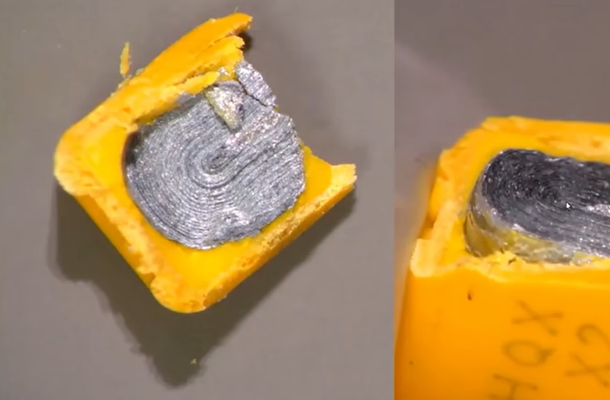
A self-healing capacitor is a power capacitor that uses a single layer of polypropylene film as the medium and a thin layer of metal evaporated on the surface as the conductive electrode.
After electrical breakdown occurs in the capacitor, the breakdown point can quickly restore insulation to ensure the safe operation of the power capacitor.
This self-healing process is due to the fact that when excessive voltage is applied, the electrical weakness of the polypropylene film is broken down, the impedance at the breakdown point is significantly reduced, and the current density flowing through increases sharply, causing the metallized coating to generate high heat, causing the breakdown point to The surrounding metal conductors quickly evaporate and escape, forming a blank area of the metal coating, and the breakdown point automatically restores the insulation. Self-healing power capacitors have the advantages of small size, light weight, large capacity, high reliability, and long life, and are widely used in power systems.
The working principle of self-healing capacitors is based on the joint action of self-healing dielectric and capacitor structure. Self-healing dielectric is composed of a combination of metal foil and polypropylene film and has excellent self-healing properties.
When the capacitor is subject to breakdown or local failure caused by external factors, the self-healing dielectric can automatically recover and isolate the fault point, thereby ensuring the normal operation of the capacitor.
The structure of a self-healing capacitor usually includes metal foil electrodes, polypropylene film as a dielectric, and insulating oil filling. Under normal operating conditions, current passes through the dielectric layer between the metal foil electrode and the polypropylene film, producing a capacitive effect and storing electrical energy. When breakdown or failure occurs in the dielectric layer inside the capacitor, the self-healing dielectric can respond quickly and form a high-impedance area around the breakdown point to prevent the flow of current, thus automatically isolating the fault point. This process is realized by the self-healing characteristics of the self-healing dielectric, which can avoid short circuit or open circuit of the capacitor and maintain the normal operation of the capacitor.
The self-healing process of self-healing capacitors is transient and usually only takes a few microseconds to tens of microseconds. Therefore, self-healing capacitors have high reliability, stability and safety, and can adapt to the complex environment and various operating conditions of the power system. In power systems, self-healing capacitors are widely used in reactive power compensation, harmonic suppression, voltage regulation and other fields, providing an important guarantee for the stable operation of the power system.
In general, the working principle of self-healing capacitors is based on the excellent performance of self-healing dielectrics and the reasonable design of the capacitor structure. Through the self-healing process, automatic isolation and repair of faults are achieved, maintaining the normal operation of the capacitor and improving the reliability of the power system. sex and stability.
The difference between self-healing capacitors and non-self-healing capacitors
The difference between self-healing capacitors and non-self-healing capacitors is mainly reflected in the following aspects:
Self-healing ability: Self-healing capacitors have self-healing ability and can repair themselves when breakdown occurs, ensuring the normal operation of the capacitor. Non-self-healing capacitors do not have this ability. Once they break down, they will cause a short circuit and cause damage to the capacitor.
Structure: The structure of the self-healing capacitor is relatively simple. Polypropylene film is usually used as the medium. The metallized film is thin and has a large square resistance. The structure of non-self-healing capacitors is more complex. Aluminum foil or aluminum film is usually used as the electrode, and the dielectric materials are also diverse.
Size and weight: Self-healing capacitors have the advantages of small size and light weight, and are easy to install and use. Non-self-healing capacitors, on the other hand, are generally larger and heavier, making them less suitable for use in environments with limited space.
Operating temperature range: Self-healing capacitors have a wide operating temperature range and can operate stably in high temperature environments. Non-self-healing capacitors are easily affected by temperature and have a narrow operating temperature range.
Price: The price of self-healing capacitors is relatively low because of their low manufacturing costs. Non-self-healing capacitors are more expensive because their manufacturing process is more complex.
Self-healing capacitors and non-self-healing capacitors each have their own advantages and disadvantages, and the choice of which capacitor to use needs to be determined based on actual needs. In situations where high reliability and stability are required and operation in high temperature environments is required, self-healing capacitors are a better choice; in situations where low cost, smaller size and weight are required, non-self-healing capacitors may be more popular. welcome.
Self-Healing Material – Analysis on the principle of self-healing material repair
Self-Healing Material – Video explaining the application of self-healing materials – Self-healing capacitors – Analysis on the principle of self-healing material repair
What are the disadvantages of self-healing capacitors
Disadvantages of self-healing capacitors include:
There are certain disadvantages during operation, which require special design to avoid. In general, the thinner the capacitor’s metallized film, the better its self-healing performance will be. However, the thinner the metallized film, the current carrying capacity of the compensation capacitor will be greatly reduced. In the long run, the capacitor will have the problem of rapid capacity attenuation due to reasons such as excessive operating temperature. Therefore, it is recommended that those self-healing capacitors with thickened metallized film edges be preferred to ensure stable operation of the capacitor in high current or high temperature environments.
Excessive oil leakage will lead to a decrease in the heat dissipation performance and voltage resistance of the capacitor, and may even affect the normal use of the capacitor.
Self-healing capacitors have high operational reliability and good capacitive performance, which can improve the stability and reliability of the power system, reduce power loss, and improve power supply quality. However, in practical applications, it is necessary to pay attention to its shortcomings and take corresponding measures to avoid them.
What are the advantages of self-healing capacitors
Advantages of self-healing power capacitors include:
Small size and light weight, saving space and easy to install.
Large capacity, able to meet the needs of large-capacity compensation.
High reliability, using self-healing technology, which can ensure that the capacitor automatically repairs faults during operation and improves operational reliability.
Long life. Due to the use of self-healing technology, the capacitor can withstand multiple overvoltage and overcurrent impacts, thus extending the service life.
Low maintenance costs. Due to the high reliability of self-healing power capacitors, the frequency of repairs and replacements can be reduced, thereby reducing maintenance costs.
The reactive power compensation effect is good, which can increase the power factor, improve voltage quality, and reduce line losses and transformer losses.
Self-healing power capacitor is a high-performance, high-reliability power electronic component with wide application prospects in power systems.
What are the advantages of self-healing capacitors compared with ordinary capacitors
The main advantage of self-healing power capacitors over ordinary power capacitors lies in their self-healing function. When the capacitor is impacted by an external voltage that is too high or too low, the self-healing power capacitor can repair itself and return to normal working condition. This self-healing ability is achieved by the self-healing material inside the capacitor.
Once the capacitor suffers a voltage shock, the self-healing material can quickly fill the insulation defects in the capacitor and prevent the current from continuing to flow, thereby avoiding damage to the capacitor.
This self-healing function makes self-healing capacitors extremely reliable and stable in high-voltage applications and complex circuits, and can maintain stable performance during long-term operation.
In contrast, ordinary power capacitors do not have a self-healing function. Once the insulation is damaged, they need to be replaced or repaired, so their reliability and stability are relatively low. Self-healing power capacitors also have a longer service life, which can reduce the frequency of replacement and maintenance and reduce maintenance costs.
In addition, self-healing power capacitors have relatively small losses and will not be damaged by multiple overvoltage and overcurrent impacts, so their operation stability and reliability are higher.
Self-healing power capacitors have higher performance and reliability than ordinary power capacitors, which can ensure the stable operation of the power system and reduce losses and maintenance costs.
Under what circumstances should self-healing power capacitors be used
It is recommended to use self-healing power capacitors under the following circumstances:
It is necessary to improve the power factor of the power system, improve voltage quality, and reduce line losses and transformer losses.
Situations where harmonics and clutter signals in the power system need to be suppressed to ensure power quality.
Where it is necessary to operate in harsh environments such as high temperature and high humidity for a long time.
Situations where the reliability and stability of capacitors are required and stable performance needs to be maintained for a long time.
Under the above circumstances, it is recommended to choose self-healing power capacitors to improve the stability and reliability of the power system and reduce losses and maintenance costs.
What models are there of self-healing power capacitors
There are many types of self-healing power capacitors, some common ones include:
BZMJ series self-healing low-voltage shunt capacitors: This series of capacitors are suitable for AC power systems with a frequency of 50Hz or 60Hz as electrical equipment to increase power factor, improve power quality, and save energy and reduce consumption.
BSMJ series self-healing low-voltage shunt capacitors: This series of capacitors are made of metallized polypropylene film material, which has self-healing properties and can effectively limit the short-circuit current of internal components.
BZMJS series self-healing low-voltage shunt capacitors: This series of capacitors is suitable for low-voltage power distribution systems and has the advantages of small size, long life, and strong anti-harmonic ability.
BKMJ series self-healing high-voltage shunt capacitors: This series of capacitors is suitable for high-voltage power systems and can provide large-capacity reactive power compensation, increase power factor and improve power quality.
In addition, there are some other models of self-healing power capacitors, such as BSMJX series, BCSMJ series, etc. Different types of self-healing power capacitors have different characteristics and usage occasions, and should be selected according to specific needs.
What is the price range of self-healing capacitors in China
The price of self-healing capacitors varies depending on factors such as model, specification, brand, and there is no unified standard. Generally speaking, the price of self-healing capacitors ranges from tens to hundreds of yuan.
In the United States, the prices of self-healing capacitors also vary greatly, and there is no unified standard. Generally speaking, the price range of self-healing capacitors ranges from tens to hundreds of dollars.
It should be noted that these prices are for reference only, and actual prices may vary due to market supply and demand, purchase volume, promotions and other factors. When choosing a self-healing capacitor, you should comprehensively consider its performance, quality, price and other factors to choose the product with the best price/performance ratio.
Is there a problem with the slightly bulging shell of the self-healing capacitor
Even if the self-healing capacitor shell bulges slightly, it indicates that there may be a problem with the capacitor. It is best to investigate the cause immediately, observe the operating status of the capacitor at all times, and replace it in time.
What are the consequences of a bulging capacitor
Reduce capacitor performance
If a self-healing power capacitor bulges, it means that its internal components are damaged or failed, which will not only cause the capacitance value to decay, but also cause the capacitor’s performance to decline.
Causing other problems
Bulging capacitors will cause other capacitors to malfunction, and the failure rate will also be greatly increased. If not replaced in time, bulging capacitors may cause short circuits, explosions and other dangerous situations, which in serious cases will pose a serious threat to the company’s economic losses and the personal safety of staff.
Causes of capacitor bulge
Long-term over-voltage and over-current operation of self-healing capacitors will cause the temperature of the capacitor to rise seriously, the pressure difference between the inside and outside of the casing to be large, and then the capacitor will suffer from bulging failure.
Factors such as excessive operating environment temperature will also cause the capacitor dielectric to age and internal components to fail. These failures will cause gas or expanding substances to be produced inside the power capacitor, causing the outer casing to bulge.
How to avoid capacitor bulge failure
Choose high-quality capacitors: When purchasing, you should choose better-quality self-healing capacitor products provided by big brands, which can ensure the reliability of capacitor quality and performance to a certain extent.
Use capacitors correctly: The operating temperature and operating voltage of self-healing power capacitors should not exceed the specified range to avoid over-voltage or over-current conditions; daily use and operation must comply with relevant guidelines.
Regular inspection and maintenance: Regularly check the status of the capacitor, including appearance, bulging, and monitoring of capacitor performance. Once a capacitor is found to have bulges or other abnormalities, it should be stopped immediately and repaired or replaced.
Ensure good ventilation and heat dissipation: Reasonable heat dissipation and ventilation should be considered when the capacitor is running to avoid over-temperature operation.
What are the application scenarios of self-healing capacitors
Self-healing capacitors are widely used in various scenarios of power systems, mainly including the following aspects:
Power system reactive power compensation: Self-healing power capacitors can provide large-capacity reactive power compensation, improve the power factor of the power system, improve voltage quality, and reduce line losses and transformer losses.
Harmonic suppression: Self-healing power capacitors have a filtering function and can effectively absorb harmonics and clutter signals in the power system to ensure power quality.
In the industrial field, self-healing power capacitors can be used for speed control of motors, filtering and power factor correction of power electronic equipment, etc.
In the field of information technology, self-healing power capacitors can be used in equipment such as data centers and communication base stations to improve their stability and reliability.
In AC power supply, self-healing power capacitors can be used to absorb various noises and interferences to ensure the DC stability of the power supply output.
Self-healing power capacitors are widely used in various fields of power systems, which can improve the stability and reliability of the system, reduce losses, and improve the quality of power supply.
The top 4 well-known self-healing power capacitor manufacturers in the world
Which of the world’s well-known self-healing power capacitor manufacturers are recommended? The world’s most well-known self-healing power capacitor manufacturers include:
Germany’s EPCOS/EPCOS AG: It is a world-famous capacitor manufacturer. Its products include electrolytic capacitors, capacitor components, inductors, ceramic capacitors, etc., which are widely used in communications, consumer electronics, industrial automation, and automotive electronics. and other fields.
VISHAY/VISHAY Intertechnology of the United States: It is one of the world’s largest passive component manufacturers. Its products include resistors, capacitors, inductors, etc., which are widely used in automobiles, industry, medical, communications and other fields.
Japan’s Panasonic/Panasonic Corporation: It is a world-renowned manufacturer of electronic products. Its products include capacitors, batteries, electronic components, etc., which are widely used in home appliances, automobiles, industry and other fields.
Samsung/Samsung Electronics of South Korea: It is a world-renowned manufacturer of electronic products. Its products include smartphones, TVs, refrigerators, washing machines, etc. It also produces various electronic components, of which capacitors are one of the important products.
These manufacturers have high reputation and market share, and their products have certain guarantees in terms of performance, quality, reliability, etc. When selecting a self-healing power capacitor manufacturer, comparison and selection should be made based on specific needs.
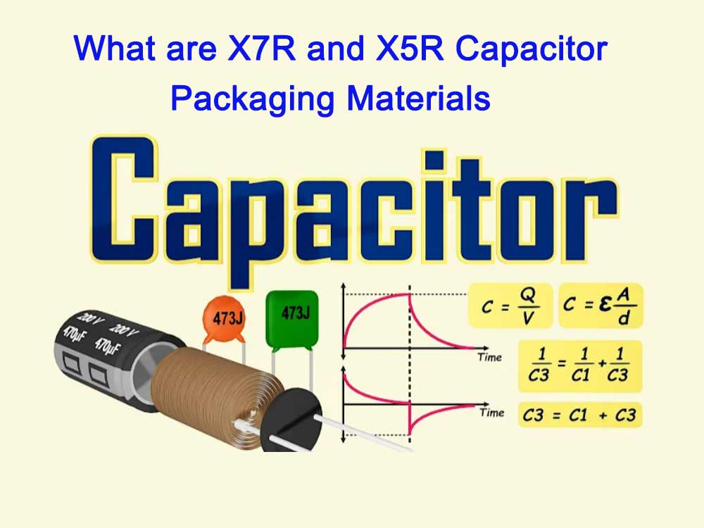
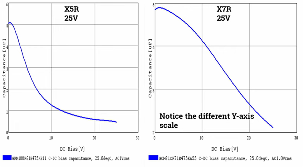
X7R and X5R capacitor packaging material characteristics
They have different characteristics:
X7R capacitor is a strong dielectric, so it can produce capacitors with larger capacity than NPO dielectric.
X5R capacitors have a high dielectric constant and are often used to produce large-capacity capacitor products with larger specific volumes and higher nominal capacities.
Difference between X7R, X5R, X8R, Z5U,Y5V, X7S, C0G Capacitor dielectrics – This video explains some of the points related to Ceramic capacitors dielectrics. How the Ceramic capacitors are categorized and what the 3 digit notations mean according to the EIA-RS-198 standard. After watching this video you will understand what are the differences between X7R,X8R,X5R,X7S, C0G/COG,NPO Y5V,Z5U capacitors
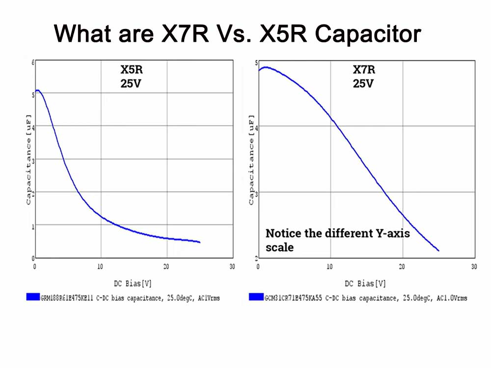
In practical applications, the performance of X7R capacitors and X5R capacitors are also different:
The performance of X7R capacitors is relatively stable. With changes in temperature, voltage and time, its unique performance does not change significantly. It is a stable capacitor material type and is used in DC blocking, coupling, bypass, filter circuits and applications with high reliability requirements. In medium and high frequency circuits.
The capacity stability of X5R is slightly inferior to that of X7R. Capacity and loss are more sensitive to test conditions such as temperature and voltage. It is mainly used in oscillation, coupling, filtering and bypass circuits in electronic machines.
In addition, the application temperature range of X7R and X5R is also different. The operating temperature range of X7R is -55℃~+125℃, while the operating temperature range of X5R is -55℃~+85℃.
X7R and X5R packaging materials are widely used in the field of multilayer ceramic chip capacitors. The specific choice of material depends on the actual application requirements.
What are the disadvantages of the X7R and X5R packaging materials
The main disadvantages of X7R and X5R packaging materials are as follows:
X7R packaging material: Although X7R has a higher dielectric constant and lower dielectric loss, its capacity stability is poor and is easily affected by test conditions such as temperature and voltage. In addition, the X7R also has lower mechanical strength and reliability.
X5R packaging material: X5R has a low dielectric constant and dielectric loss, so its capacity is small and is not suitable for applications requiring high capacity. In addition, the reliability of the X5R is not as high as that of the X7R.
It should be noted that these shortcomings do not mean that the X7R and X5R packaging materials are not available, but that they still need to be improved in some aspects. In practical applications, appropriate packaging materials can be selected according to specific needs.
What are the application scenarios of X7R and X5R packaging materials
The application scenarios of X7R and X5R packaging materials mainly depend on their performance characteristics.
X7R packaging material: Because X7R has the advantages of good temperature stability, low dielectric loss, and large capacity, it is suitable for application scenarios that require high temperature changes. In addition, due to its high mechanical strength and reliability, X7R is widely used in various medium and high-frequency circuits in the electronics industry, such as DC blocking, coupling, bypass, filter circuits, etc., especially in some applications with higher reliability requirements. Scenes.
X5R packaging material: X5R packaging material has a relatively high dielectric constant, so it is often used to produce large-capacity capacitor products with larger specific volume and higher nominal capacity. Because of its good capacity stability and sensitivity to test conditions such as temperature and voltage, it is mainly used in oscillation, coupling, filtering and bypass circuits in electronic machines. X5R packaging materials are more suitable for applications requiring high frequency applications or high capacity requirements.
X7R and X5R packaging materials are widely used in different application scenarios, and the appropriate packaging materials need to be selected according to specific needs.
What are the insulation dielectric constant and dielectric loss of X7R capacitor and X5R capacitor
The specific values of insulation dielectric constant and dielectric loss of X7R and X5R are as follows:
The insulation dielectric constant of X7R is generally between 10,000 and 20,000, while the dielectric loss is less than 2%.
The insulation dielectric constant of X5R is generally between 8000 and 15000, and the dielectric loss is less than 3%.
Please note that these values may vary depending on the manufacturer, material composition and manufacturing process. Therefore, when selecting X7R and X5R packaging materials, in addition to paying attention to dielectric constant and dielectric loss, it is also necessary to comprehensively consider their application needs and reliability requirements.
What are the dielectric constants of X7R capacitors and X5R capacitors
The dielectric constants of X7R capacitors and X5R capacitors are 3000 to 6000 and 8000 to 12000 respectively.
Which type of material encapsulates capacitors with better performance
Overall, the X7R capacitor packaging material has better capacitor performance.
Temperature stability: X7R has better temperature stability and is suitable for high temperature environments.
Capacity stability: X7R has high capacity stability when temperature and voltage change.
However, there are also opinions that the capacitor performance of X5R is better, and the specific choice of packaging material should be determined based on the actual application requirements.
What are the performance indicators of capacitor X7R and capacitor X5R packaging materials
The performance indicators of capacitor X7R and capacitor X5R packaging materials mainly include capacitance, equivalent series resistance (ESR), temperature characteristics, loss tangent value, etc.
Capacitance: The capacitance ranges of X7R and X5R capacitors are different and need to be selected according to actual needs.
Equivalent Series Resistance (ESR): This is an important parameter to measure the performance of a capacitor. Lower ESR means better performance.
Temperature characteristics: The temperature characteristics of X7R and X5R capacitors are different and need to be selected according to actual needs.
Loss tangent value: This is a parameter that measures the loss of the capacitor. Lower loss tangent value means lower loss.
Generally speaking, the performance indicators of X7R and X5Rpackaging materials are relatively similar, but the specific values and ranges are different. When selecting packaging materials, these factors need to be considered based on actual needs.
Which one has greater capacity, X5R capacitor or X7R capacitor
Generally speaking, X7R capacitors have larger capacitances and are suitable for applications requiring higher capacitance values. X5R, on the other hand, has a relatively small capacitance and is more suitable for applications with less stringent capacitance value requirements.
However, some people believe that X5R capacitors have a higher dielectric constant and therefore can store more charges. They are often used to produce large-capacity capacitor products with larger specific volumes and higher nominal capacities. The X7R capacitor is a strong dielectric, so it can produce capacitors with a larger capacity than NPO dielectric. This means that X7R capacitors are more suitable in applications requiring high capacitance.
Therefore, the capacity of X5R capacitors and X7R capacitors is not absolute, and the specific selection needs to be determined based on actual application requirements.
Which one is safer, X7R capacitor or X6R capacitor
Both X7R capacitors and X6R capacitors are safer, but which one is safer needs to be considered from different perspectives.
Considering overload protection: X6R has better overload protection performance and can withstand higher voltage and current. Therefore, X6R may be safer for some application scenarios that need to withstand larger transient currents.
Considering temperature stability: X7R has better temperature stability and can maintain stable performance in a wider temperature range. Therefore, for some application scenarios that need to work at higher or lower temperatures, X7R may be more suitable. Safety.
To sum up, both X7R and X6R capacitors have high safety. The specific choice of capacitor should be decided based on the actual application requirements. If you need to withstand larger transient currents, you can choose X6R; if you need to work at higher or lower temperatures, you can choose X7R.
What is the difference between the packaging materials of X7R capacitors and X5R capacitors
The main differences between the X7R and X5R packaging materials are their dielectric constant and temperature stability.
Dielectric constant: X7R has a strong dielectric, while X5R has a higher dielectric constant. This means that X5R can store more charges, so it is often used to produce large-capacity capacitor products with larger specific capacitance and higher nominal capacity.
Temperature stability: X7R capacitor performance is relatively stable. With changes in temperature, voltage and time, its unique performance does not change significantly. It is a stable capacitor material type and is used in DC isolation, coupling, bypass, filter circuits and reliable In medium and high frequency circuits with higher performance requirements. The capacity stability of X5R is slightly inferior to that of X7R. Capacity and loss are more sensitive to test conditions such as temperature and voltage. It is mainly used in oscillation, coupling, filtering and bypass circuits in electronic machines.
X7R and X5R packaging materials are widely used in the field of multilayer ceramic chip capacitors. The specific choice of material depends on the actual application requirements.
What is the price of packaging materials for Capacitor X7R and Capacitor X5R
The prices of X7R and X5R packaging materials are relatively stable, but are affected by many factors and the specific prices will vary. Generally speaking, the price of X7R packaging materials is relatively high, while the price of X5R packaging materials is relatively low.
The following are factors that may affect the price of X7R and X5R packaging materials:
Market demand: Market demand is one of the important factors affecting prices. If the market demand is large, the price will rise accordingly; if the market demand is small, the price will fall accordingly.
Quality: The prices of X7R and X5R packaging materials of different qualities will also be different. High-quality packaging materials usually have higher performance indicators and more stable performance, so the price is relatively high.
Brand: Well-known brands of X7R and X5R packaging materials usually have higher reputation and quality assurance, so the price is relatively high.
Supply situation: If the supply of X7R and X5R packaging materials is tight, the price will rise accordingly; if the supply is sufficient, the price will fall accordingly.
To sum up, the prices of X7R and X5R packaging materials are relatively stable, but are affected by many factors. When selecting packaging materials, in addition to considering price factors, it is also necessary to comprehensively consider factors such as performance, quality, brand and supply.
X7R capacitor Vs. X5R capacitor
Application of X7R capacitor and X5R capacitor packaging materials in automotive electronics
Both X7R and X5R packaging materials are used in automotive electronics, but the specific application scenarios are different.
X7R packaging materials are mainly used in power supply, LED, UPS, automotive electronics and other fields. In these fields, high-capacity capacitors are required to provide stable power and signals, as well as high voltage and temperature resistance. The high dielectric constant and stability of the X7R packaging material make it ideal for these applications.
In contrast, X5R packaging materials have relatively few applications in automotive electronics. This is mainly because the X5R packaging material has a low dielectric constant and a small capacity, making it unsuitable for applications requiring high capacity.
To sum up, X7R packaging materials have wider applications in automotive electronics, while X5R packaging materials have relatively few applications. When selecting packaging materials, it is necessary to select the appropriate packaging material based on specific application requirements.
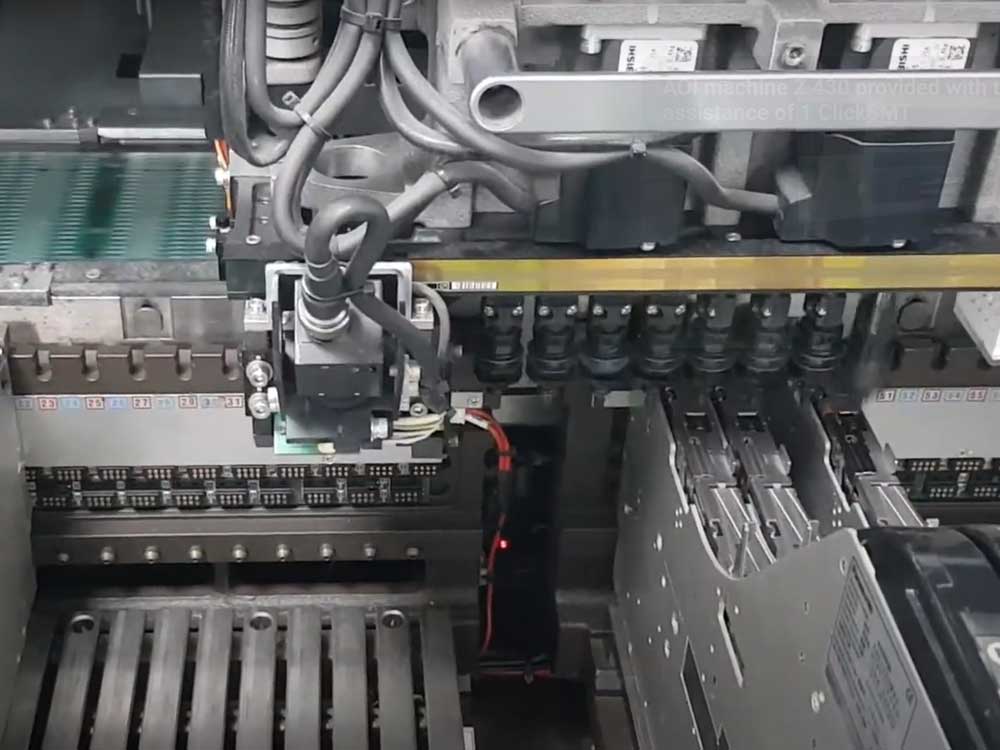
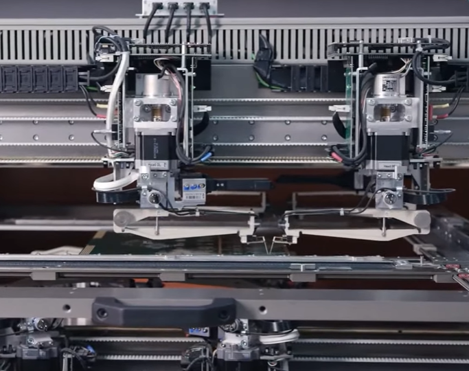
SMT (Surface Mount Technology) automatic tape splicing equipment is a key automation technology in electronic manufacturing.
It is mainly used for sorting, counting and detecting SMT disc tapes. The application of this technology makes the electronic manufacturing process more efficient and accurate, and promotes the progress of the entire electronics industry.
Guangdong Guoyu Technology SMT anti-static splicing tape equipment part
One of the primary functions of this equipment is the sorting of SMT disc tapes. In the traditional electronics assembly process, manual sorting of material strips is relatively inefficient and contains errors. However, the automatic splicing strip equipment can quickly and accurately identify and sort disk-shaped materials through advanced vision systems and robotic arm technology.
Various components on the belt. This not only improves production efficiency, but also reduces the possibility of human error and provides a reliable foundation for subsequent production links.
Secondly, this equipment plays a key role in counting SMT disc tapes. Through precise counting functions, automatic tape splicing equipment can quickly and accurately confirm the number of components in each tape. This helps ensure that insufficient or redundant components do not occur during assembly, thereby improving product quality and reliability.
In addition, the SMT anti-static splicing tape equipment also has the function of detecting components. Through advanced sensors and detection technology, the equipment can detect key information such as the quality, orientation and location of components. This helps to detect possible defects or anomalies in time, ensures that only components that meet standards are used for assembly, and improves the stability and controllability of the entire production line.
The advantage of this automation technology lies not only in improving production efficiency and product quality, but also in its saving of human resources. Compared with traditional manual operation, SMT anti-static splicing tape equipment is not only faster and more accurate, but also can run continuously, reducing production risks caused by human factors.
The widespread application of SMT anti-static splicing tape equipment has enabled the electronics manufacturing industry to make significant progress in improving production efficiency, reducing costs, and improving product quality.
This advanced technology plays an irreplaceable role in meeting the needs of the modern electronics industry for efficient, precise and reliable production, laying a solid foundation for the future development of the electronics manufacturing industry.
Overview of the process flow of SMT anti-static splicing tape equipment
In Surface Mount Technology (SMT), anti-static splicing tape equipment is an important auxiliary equipment, mainly used to prevent static electricity from damaging electronic components.
The process flow mainly includes the following steps: splicing tape supply, splicing tape positioning, electronic component placement, welding, inspection and testing.
Supply of splicing tape: The splicing tape is pulled out from the reel and passes through the guide wheel and tension wheel to maintain a certain tension to ensure its stable position during the production process.
Splice tape positioning: Before placing electronic components on the circuit board, the splice tape is accurately placed at a specific location on the circuit board to secure the electronic components.
Electronic component placement: Use an automatic or semi-automatic component placement machine to place electronic components on the splicing tape.
Welding: Use welding techniques such as hot melt welding or ultrasonic welding to connect electronic components to circuit boards.
Inspection and testing: Conduct quality inspection and performance testing on the soldered circuit board to ensure that it meets the preset quality standards.
Each step is critical to the quality and reliability of the final product, so the operating parameters and process conditions of each link need to be strictly controlled.
Detailed introduction to the process flow of anti-static splicing tape equipment
Supply of splicing tape: The splicing tape is pulled out from the reel, passes through the guide wheel and tension wheel, and enters the production area. The function of the guide wheel and tension wheel is to control the speed and tension of the splicing belt to ensure its stability during the production process. In addition, in order to prevent static electricity from damaging electronic components, an anti-static coating is usually added to the splicing tape.
Splice tape positioning: Before electronic components are placed on the circuit board, the splice tape is accurately placed at a specific location on the circuit board. This step is usually completed by a positioning system, which can adjust the position of the splicing strip according to the reference point on the circuit board to ensure the accuracy of component placement. At the same time, in order to ensure production efficiency, the positioning system should also have the ability to adjust the position quickly and accurately.
Electronic component placement: Use an automatic or semi-automatic component placement machine to place electronic components on the splicing tape. The component placement machine can accurately place electronic components on the splicing tape according to preset data and programs. In order to ensure the accuracy and stability of component placement, component placement machines need to be calibrated and maintained regularly.
Welding: Use welding techniques such as hot melt welding or ultrasonic welding to connect electronic components to circuit boards. During the welding process, attention needs to be paid to the control of parameters such as temperature, time and pressure to ensure welding quality. At the same time, in order to prevent the impact of static electricity on welding, corresponding anti-static measures need to be taken, such as grounding and using an anti-static workbench.
Inspection and testing: Conduct quality inspection and performance testing on the soldered circuit board to ensure that it meets the preset quality standards. Various inspection tools and technologies are required during the inspection and testing process, such as visual inspection, electrical performance inspection, etc. At the same time, defective products also need to be traced and processed to reduce the defective rate.
In general, the SMT anti-static splicing tape equipment process requires strict control of the operating parameters and process conditions of each link to ensure the quality and reliability of the final product.
In actual production, adjustments and optimizations need to be made according to specific circumstances to improve production efficiency and reduce costs.
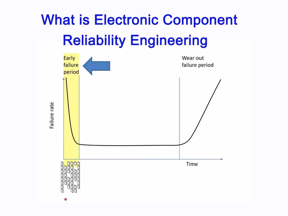
Electronic components are the smallest units that constitute electronic systems or electronic equipment, and their reliability directly affects the performance and life of the entire system or equipment. Therefore, electronic component reliability engineering has become an important research field.
This project covers the research on the physical properties, chemical properties, and electrical properties of electronic components, and also involves considerations of environmental factors, usage conditions, manufacturing processes, etc.
Failure mechanism and life prediction of components: Study the failure mechanism of electronic components under different environmental conditions, establish a component life prediction model, and provide a basis for the reliability design and evaluation of components.
Reliability design and analysis: Improve the reliability and stability of components through reliability design, analysis and optimization. This includes circuit design, packaging design, heat dissipation design, etc.
Reliability testing and evaluation: Through various environmental tests, life tests and reliability evaluations, the performance and reliability level of components under actual use conditions are tested.
Reliability management: Establish a component reliability management system, formulate corresponding standards and specifications, and effectively manage the procurement, acceptance, and use of components.
Application and promotion of reliability technology: Apply reliability engineering to actual production to improve the performance and lifespan of electronic products and promote the sustainable development of the electronics industry.
What are the advantages of electronic component reliability engineering
The advantages of electronic component reliability engineering mainly include the following points:
Improve product quality: Through the application of electronic component reliability engineering, the quality and reliability of electronic products can be ensured, the failure rate of products during production, use and maintenance can be reduced, and the overall performance and life of the product can be improved.
Enhance market competitiveness: In the fiercely competitive electronic product market, products with high reliability are more competitive. Consumers are more inclined to choose products with high reliability and stable performance, so electronic component reliability engineering can improve the market competitiveness of products.
Reduce maintenance costs: Since electronic component reliability engineering emphasizes comprehensive quality control and reliability management of products, it can reduce maintenance and replacement costs during product use. This not only reduces production costs, but also increases the added value of the product.
Promote technological progress: Electronic component reliability engineering involves knowledge from multiple disciplines and fields, and requires continuous technological research and development and innovation. This can promote technological progress in related fields and promote the sustainable development of the entire electronics industry.
Enhance safety: Through the application of electronic component reliability engineering, the safety and stability of electronic products can be improved, avoiding accidents or failures during product operation, and ensuring the personal safety of users.
From the above explanation, we can see that electronic component reliability engineering has many advantages, including improving product quality, enhancing market competitiveness, reducing maintenance costs, promoting technological progress, and enhancing safety. Therefore, it is very necessary to promote and apply electronic component reliability engineering in the electronics industry.
What are the disadvantages of electronic component reliability engineering
The shortcomings of electronic component reliability engineering mainly include the following points:
High technical requirements: Electronic component reliability engineering requires knowledge in multiple disciplines and fields, and has high technical requirements. In order to meet reliability requirements, advanced processes, materials and design methods need to be adopted, which requires a lot of technical investment and R&D work.
Higher cost: Due to high technical requirements, the cost of reliability engineering of electronic components is also relatively high. A large amount of manpower, material and financial resources need to be invested in research and development, production, testing and other aspects, resulting in increased costs.
Long cycle: The R&D and production cycle of electronic component reliability engineering is relatively long. In order to ensure the reliability and stability of components, a large number of experiments and tests need to be carried out, which requires a lot of time and manpower. In addition, during the production process, process parameters and quality standards also need to be strictly controlled, which will also extend the production cycle.
High risk: Electronic component reliability engineering involves the quality and reliability of the product. Once a problem occurs, it may have a major impact on the entire system or equipment. Therefore, strict quality control measures need to be taken during the R&D and production processes to reduce risks.
Although electronic component reliability engineering has the above shortcomings, its importance and application value are also constantly increasing with the continuous advancement of technology and the increasing application requirements.
Through continuous technological innovation and optimization, these shortcomings can be overcome, the reliability and stability of electronic components can be improved, and strong support can be provided for the development of the electronics industry.
What is the difference between the definitions of electronic component reliability engineering and reliability engineering
There are certain differences in the definitions between electronic component reliability engineering and reliability engineering.
Electronic component reliability engineering mainly focuses on the reliability issues of electronic components, including failure mechanisms, life prediction, reliability design, reliability testing and evaluation of electronic components, etc.
It is the application and extension of reliability engineering in the field of electronic components, focusing on solving problems such as performance, lifespan and reliability of electronic components under various environmental conditions.
Reliability engineering is an interdisciplinary engineering discipline involving multiple disciplines and fields. It mainly studies the failure causes, failure modes and failure mechanisms of products, and how to improve the reliability and stability of products.
Reliability engineering involves the knowledge of mathematics, physics, engineering, quality management and other disciplines, aiming to provide reliability and stability guarantee for product design and production.
Therefore, electronic component reliability engineering is a branch of reliability engineering, which mainly focuses on the reliability and stability of electronic components and provides guarantee for the quality and performance of electronic products.
Application areas of electronic component reliability engineering
Aerospace: In the aerospace field, electronic components work in harsh environments and require extremely high reliability. Therefore, electronic component reliability engineering has broad application prospects in the aerospace field.
Automotive electronics: Automotive electronic systems have high requirements for reliability and safety. Electronic component reliability engineering can provide strong support for the design and production of automotive electronic systems.
Communication and network: Communication and network equipment need to operate stably for a long time, and have high requirements on the reliability and stability of components. Electronic component reliability engineering can provide technical support for the design and production of communication and network equipment.
Industrial control: Electronic equipment used in the field of industrial control needs to have high reliability and stability to ensure the normal operation of the production process. Electronic component reliability engineering can provide technical support for the design and production of industrial control equipment.
Smart home: Smart home systems need to operate stably for a long time and are involved in people’s daily lives, so they have high requirements for the reliability and stability of electronic components. Electronic component reliability engineering can provide technical support for the design and production of smart home devices.
Development Trends in Reliability Engineering of Electronic Components
Application of new materials and new processes: With the development of new materials and new processes, the reliability of electronic components has been further improved. In the future, new materials and new processes will be more widely used, providing more possibilities for the development of reliability engineering of electronic components.
Application of intelligent and automated technology: Intelligent and automated technology can greatly improve the efficiency and accuracy of electronic component reliability engineering. In the future, intelligent and automation technology will be more widely used in electronic component reliability engineering.
Interdisciplinary cooperation and exchange: Electronic component reliability engineering involves knowledge from multiple disciplines and fields, requiring cooperation and exchanges between experts in different fields. In the future, interdisciplinary cooperation and exchanges will become more frequent and closer, promoting the rapid development of electronic component reliability engineering.
Sustainable development and environmental protection requirements: As society’s requirements for sustainable development and environmental protection increase, electronic component reliability engineering will pay more attention to environmental protection and energy-saving design. In the future, environmental protection and energy-saving design will become an important development direction of electronic component reliability engineering.
Standardization and standardized development: In order to standardize the development and application of electronic component reliability engineering, it is necessary to formulate corresponding standards and specifications. In the future, the degree of standardization and normalization of electronic component reliability engineering will be further improved.
To sum up, electronic component reliability engineering is a highly comprehensive engineering field involving knowledge from multiple disciplines and fields.
With the continuous development of science and technology and the continuous improvement of application requirements, electronic component reliability engineering will face broader development prospects and challenges.
In the future, we need to further in-depth research and exploration to promote continuous innovation and development of electronic component reliability engineering.
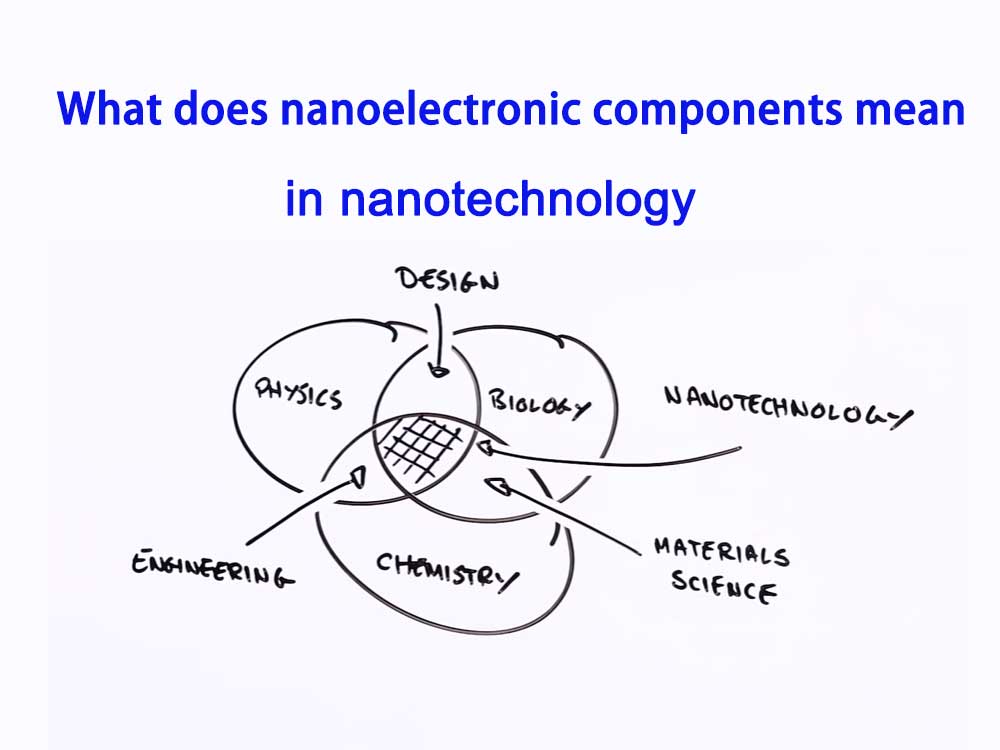
In nanotechnology, nanoelectronic components refer to electronic components manufactured using nanotechnology, and their dimensions are usually at the nanometer level (ie, between 1 nanometer and 100 nanometers).
Due to their extremely small size, nanoelectronic components have many unique properties and advantages, and therefore have broad application prospects in the field of electronic technology in the future.
Overview of Nanoelectronic Components
The core technology of nanoelectronic components is nanotechnology, which involves knowledge from multiple disciplines such as physics, chemistry, and materials science.
At the nanometer level, the properties of matter undergo significant changes, which provides new possibilities for the design and manufacture of electronic components.
Nanotechnology: Nanoelectronics
Compared with traditional electronic components, nanoelectronic components have higher performance, lower power consumption and smaller size, and are therefore considered to be one of the key technologies for the next generation of electronic technology.
At present, people have used nanoelectronic materials and nanolithography technology to develop many nanoelectronic devices, such as electron resonance tunneling devices, resonant diodes, tripole resonance tunneling transistors, single electron transistors, metal-based, semiconductors, nanoparticles, single electron transistors, etc.
Electronic electrometer, single electron memory, single electron logic circuit, metal-based single electron transistor memory, semiconductor memory, memory made of silicon nanocrystals, nano floating gate memory, nano silicon microcrystalline thin film devices and polymer electronic devices, etc.
Nanoelectronics technology refers to related technologies that construct nano and quantum devices within the nanometer size range and integrate nano circuits to realize information calculation, transmission and processing of quantum computers and quantum communication systems. Among them, nanoelectronics devices are the current development of nanoelectronics technology. The key and core. Nowadays, nanoelectronics technology is in a period of vigorous development.
Its ultimate goal is to break through the traditional physical size and technical limits based on the latest physical theory and the most advanced process methods, and develop the potential information and structural potential of matter. According to new concepts, Design and manufacture nanodevices and construct electronic systems to achieve a revolutionary leap in the ability of electronic systems to store and process information.
Nanoelectronic devices refer to electronic devices with nanoscale scale and specific functions designed and prepared using nanoscale processing and preparation technologies, such as photolithography, epitaxy, microfabrication, self-assembly growth and molecular synthesis technology.
Nanotechnology is a high-tech discipline that studies and applies the motion patterns and characteristics of electrons, atoms and molecules within a 0.1-100um scale space. Its goal is to use single atoms and molecules to create products with specific functions.
Domestic and foreign scientific and technological circles have generally believed that nanotechnology has become the most dynamic research object in today’s research field and is very important to future economic and social development. Nanotechnology is promoting huge changes in human society. It will not only promote a revolution in human understanding, but also trigger a new industrial revolution.
Nanotechnology is a new field of science and technology that emerged in the late 20th century. It is a new high-tech subject group, including nanoelectronics, nanophotonics, nanophotonics, nanophysics, nanooptics, nanomaterials, and nanomachinery. science, nanobiology, nanometrics, nanotechnology, nanomedicine, nanomicroscopy, nanoinformation technology, nanoenvironmental engineering and nanomanufacturing, etc. It is an emerging technology that integrates basic research and application exploration.
Nanoelectronics is the detection, identification and control of the movement patterns of single quantum or quantum waves within 0.1~100nm nanostructures (quantum dots), and the study of artificial assembly and self-assembly technology of individual atoms and molecules. Research within quantum dots, The characteristics and functions exhibited by a single quantum or quantum wave are devices, circuits and systems used for the generation, transmission and exchange of information and their applications in information science and technology, nanobiology, nanometry, nanomicroscopy, nanomechanics, etc. An applied discipline, also known as quantum functional electronics.
Nanoelectronics is an important part of nanotechnology, an inevitable result of the development of traditional microelectronics, and the main driving force for the development of nanotechnology. Nanoelectronics is based on traditional solid-state electronics, using the latest physical theory and the most advanced process methods to construct electronic devices and systems according to new concepts. Nanoelectronics has the ability to develop the potential information and structure of matter at a deeper level, increasing the ability to store and process information per unit volume of matter by more than a million times, achieving a revolutionary breakthrough in information collection and processing capabilities.
Nanoelectronics is combined with optoelectronics, biology, mechanics and other disciplines to produce nanoelectronics/optoelectronic devices, molecular devices, nanoelectronic mechanical systems, nanooptoelectronic mechanical systems, micro-robots, etc., which will have an impact on human production and lifestyle. Producing a transformative impact, nanoelectronics/optoelectronics will become a key science and technology in the information age of the 21st century.
According to Moore’s Law, in the next 10 years or so, continuing to improve the storage density and computing power of computers will face severe challenges. These challenges include both theoretical physical limitations and technical process limitations. Its main manifestation is that when the size of the electronic device is on the order of microns, the electrons in it are mainly particulate. But when the size of the device is as small as nanometers, the electrons are mainly wave-like. The volatility of electrons is a quantum effect.
At this time, electronic devices will work under a completely new principle; any multi-body system has thermal statistical fluctuations. When the size of the device is reduced to the nanometer level, this thermal fluctuation will It will limit the consistency of device performance, causing the integrated chip to fail to work properly.
However, the emergence of nanoelectronics technology, nanoelectronic devices and nanoelectronics has provided new ways and opportunities for the development of microelectronics technology.
On the one hand, this can be attributed to the continuous development of microelectronics and nanotechnology; on the other hand, it can be attributed to the powerful contributions provided by microelectronics and quantum physics to the preparation, characteristics, mechanism and characterization of nanoelectronic devices over more than half a century. support.
Classification of Nanoelectronic Devices
Based on current development and predictions for the future, if the main nanoelectronic devices are further classified, nanoCMOS devices mainly include: silicon-on-insulation MOSFET, silicon-germanium heterogeneous MOSFET, low-temperature MOSFET, bipolar MOSFE T, and intrinsic silicon trench Tunnel type MOSFET, etc.; quantum effect devices include: quantum interference devices, quantum dot devices and resonant tunnel devices, and resonant tunnel devices include: lateral resonant tunnel devices, resonant tunnel transistors, resonant tunnel field effect transistors (RTEET), dual Polar quantum resonant tunnel transistors, resonant tunnel hot electron transistors, longitudinal resonant tunnel devices and tunnel barrier modulation transistors, etc.; single electron devices mainly include: single electron boxes, capacitor coupled and resistor coupled single electron transistors, single electron neural network transistors , single-electron junction array, single-electron pump, single-electron trap and single-electron revolving door, etc.; single-atom devices and single-molecule devices include: single-electron switches, single-atom point contact devices, single-molecule switches, molecular wires, quantum effect molecules Electronic devices, electrochemical molecular electronic devices, etc.
Nanosensors include
Quantum tunnel sensors and nano-biosensors; nano-integrated circuits, nano-electronic integrated circuits and nano-optoelectronic integrated circuits. Nano-memory includes: ultra-high-capacity nano-memory, ultra-high-density data memory, tunnel-type static random access memory, single-electron silicon-based MOS memory , single-electron memory, single-electron quantum memory; nano-CMOS hybrid circuits include: nano-CMOS circuits and 1-V compound semiconductor resonance tunneling effect circuits, nano-CMOS circuits and single-electron nano-switch circuits, nano-CMOS circuits and superconducting single magnetic flux quantum circuits Circuits, the marriage of nano-CMOS circuits and carbon nanotube circuits, nano-CMOS circuits and artificial atomic circuits and artificial molecular circuits, nano-CMOS circuits and DNA circuits, nano-CMOS circuits and nano-metal-based spin circuits, and other mainstream circuits, provide a basis for nanoelectronics Created a new development. Nano 1`V compound semiconductor devices and circuits refer to resonant tunnel diodes and resonant tunnel transistors and circuits. It has strong potential in the fields of high speed, high frequency and optoelectronics.
Scientists predict that in the 21st century, nanoelectronic devices, nano optoelectronic devices, nano Integrated circuits and nano-optoelectronic integrated circuits are the most promising. Sensors manufactured using nanotechnology have higher sensitivity and smaller size and can be used in medical, environmental protection, military and other fields. For example, biosensors based on single-walled carbon nanotubes can be used to detect biomolecules and cells.
Nanosingle electron devices
Many nanoelectronic devices have been developed using nanoelectronics using nanoelectronic materials and nanolithography technology, such as: electron resonance tunneling devices, electron resonance tunneling devices, resonant diodes (RTD), and three-terminal resonant tunneling transistors (RTT). ), single electron transistor (SET), single island single electron transistor (SET), metal-based SET, semiconductor SET, nanoparticle SET, multi-island SET, single electron electrometer, single electron memory (SEM), single electron logic circuit, Single electron cMOS circuit, metal-based single electron transistor (sET) memory, semiconductor SET memory, memory made of silicon nanocrystals, nano floating gate memory, single electron digital integrated circuit, single electron transistor (sET) logic integrated circuit , nano silicon microcrystalline thin film devices (such as resonant tunneling diodes (RTD)) and polymer electronic devices, etc.
nanotransistor
This is the most basic type of nanoelectronic components, with dimensions ranging from a few to tens of nanometers. Compared with traditional transistors, nanotransistors have faster switching speeds and lower power consumption, so they have broad application prospects in high-speed, low-power integrated circuits.
Electronic wave devices
Electron wave interference devices, short-line waveguide interference devices, MachZender interferometers (electrostatic interference devices), directional coupling devices, diffraction devices, quantum wire channel field effect transistors (FETs), planar superlattice FETs, electron velocity modulation FET resonant tunnels Wearing devices, etc.
The electrons in quantum wave devices are in a phase-coherent structure, and their behavior is mainly wavelike. Such devices include quantum wire transistors, quantum interference devices, resonant tunneling diode transistors, etc.
Nano solar cells
Nanostructures are used to improve the light absorption efficiency and photoelectric conversion efficiency of solar cells, with higher energy conversion efficiency and smaller size. For example, solar cells based on titanium dioxide nanorods have excellent performance.
nanomemory
Memories manufactured based on nanotechnology have higher storage density and faster read and write speeds. For example, carbon nanotube random access memory is a type of memory based on carbon nanotubes that has a storage density several orders of magnitude higher than traditional flash memory.
Preparation Technology of Nanoelectronic Devices
To prepare nanoelectronic devices and realize their integrated circuits, there are two possible ways. One is to further extend existing electronic devices and integrated circuits toward miniaturization, and research and develop processing technology with smaller line widths to process smaller electronic devices, which is the so-called “top-to-bottom” approach.
Another way is to use advanced nanotechnology and the quantum effects of nanostructures to directly form new quantum devices and quantum structure systems, which is the so-called “bottom-up” approach.
The “top-to-bottom” preparation method of nanoelectronic devices mainly refers to technologies such as optical lithography, electron beam lithography, and ion beam lithography.
“Bottom-up” preparation methods include metal-organic chemical vapor deposition, molecular beam epitaxy, atomic layer epitaxy, chemical beam epitaxy and other epitaxy technologies, scanning probe microscopy technology, molecular self-assembly synthesis technology and special ultra-fine processing technology wait.
Lithography
Optical lithography, electron beam lithography and ion beam lithography technology are collectively referred to as three-beam lithography technology.
Processing technology that transfers designed device pattern structures to semiconductor substrates. At present, as the line width of lithography technology continues to decrease, optical lithography, electron beam lithography and ion beam lithography have shown good applications in the processing fields of nano devices, nano integrated circuits, nano hybrid circuits and so on. prospects, and has begun to be applied in the processing of some nanoelectronic devices.
Optical lithography technology
Optical lithography is a technology that uses an optical system to “engrav” the large-scale integrated circuit device structure pattern on the mask onto a silicon wafer coated with photoresist using a projection method. It is now the mainstream technology for industrial semiconductor processing. In this technique, methacrylate polymers are typically used as the resist coating and a mixture of methyl isobutyl ketone and isopropyl alcohol is used as the developer.
At present, the most attracting hot spot in the international microelectronics field is the new generation of photolithography technology. Limiting the minimum line width that can be obtained by lithography is directly related to the resolution of the lithography system, and reducing the wavelength of the light source is the most effective way to improve the resolution of lithography.
Now, the light source wavelength of commercial lithography machines has entered the deep ultraviolet band from the past mercury lamp source ultraviolet band. In addition, using the interference characteristics of light and electromagnetic theory combined with in-depth analysis of exposure imaging in lithography practice, Optimizing process parameters using various wavefront technologies is also an important means to improve lithography resolution.
electron beam lithography
Electron beam lithography is a photolithography technology that uses high-energy electron beams to expose photoresist to obtain structural patterns.
Recently, the angle-limited scattered projection electron beam lithography technology developed by Lucent in the United States is attracting attention. This technology reduces the projection of the mask pattern like optical lithography, and uses special filtering technology to remove scattered electrons generated by the mask absorber.
This improves output efficiency while ensuring resolution. It should be pointed out that no matter what technology is used in lithography in the future, it will be an indispensable infrastructure for integrated circuit research and production.
Ion beam lithography
Ion beam lithography is a photolithography technology that uses ions formed after ionization of liquid atoms or gaseous atoms to expose photoresist after being accelerated by an electromagnetic field and focused or collimated by an electromagnetic lens.
Its principle is similar to that of electron beam lithography, but the de Broglie wavelength is shorter, and has the advantages of no proximity effect, small exposure field, etc. Ion beam lithography mainly includes focused ion beam lithography, ion projection lithography, etc. epitaxial technology
Metal-organic chemical vapor deposition, molecular beam epitaxy, atomic layer epitaxy and chemical beam epitaxy technology are collectively referred to as epitaxial technology. It is a nano-manufacturing technology that grows nano-films on a substrate. It can be used for silicon-based semiconductor materials for nano-integrated circuits, nanometer Semiconductor structures: Device processing and preparation.
The beam intensity is proportionally sprayed onto the heated substrate surface, and ultimately interacts with the surface for epitaxial growth of single crystal films. The baffle in front of each blast furnace is used to change the composition and doping of the epitaxial film.
According to the set program, the baffle is opened and closed, the furnace temperature is changed, and the growth time is controlled.
Compounds with different thicknesses or ternary and quaternary solid solutions with different composition ratios and their heterojunctions can be grown, thereby preparing various ultra-thin products. Microstructured materials.
In recent years, with the development of materials science, physics, chemistry and other disciplines, the research on nanoelectronic components has made significant progress.
In the laboratory, people have successfully prepared various types of nanoelectronic components and conducted in-depth research on their properties.
At the same time, with the continuous advancement of manufacturing processes, the manufacturing costs of nanoelectronic components are gradually decreasing, making their commercial applications possible.
Challenges and Prospects of Nanoelectronic Components
Although nanoelectronic components have many advantages and broad application prospects, their research and application also face many challenges.
For example, how to control the size and performance of nanoelectronic components during the manufacturing process, how to improve their stability and reliability, how to achieve mass production and commercial applications, etc.
In addition, since nanoelectronic components involve knowledge in multiple subject areas, interdisciplinary cooperation and communication are required to solve the problems.
In the future, with the continuous advancement of technology and increasing application requirements, the research and application of nanoelectronic components will usher in broader development prospects. People expect nanoelectronic components to bring smaller size, higher performance, lower power consumption and lower cost to future electronic products.
At the same time, with the improvement of environmental awareness, the concepts of green, renewable and sustainable development will also be introduced into the research and application of nanoelectronic components.
For example, using renewable energy to manufacture nanoelectronic components and realizing environmentally friendly treatment of discarded nanoelectronic components.
In general, nanoelectronic components are one of the important development directions in the field of electronic technology in the future. Although there are still many challenges and problems that need to be solved, with the continuous advancement of science and technology and the continuous improvement of application requirements, it is believed that these problems will also be effectively solved.
In the future, we look forward to more innovations and breakthroughs in the field of nanoelectronic components to contribute to the sustainable development of human society.
Recommendations for future development of nanoelectronic devices
Attention must be paid to and vigorously carried out research on nano-devices, especially nano-electronic devices and nano-optoelectronic devices.
Academician Bai Chunli once pointed out that “the level of development and application of nano-devices is an important indicator of whether we have entered the nano-era”, and pointed out that “China must pay attention to the research work on the development of nano-devices and nano-scale detection and characterization.”
According to the current status of my country’s nanotechnology development, we must vigorously advocate the research, development and application of nanodevices, especially nanoelectronic devices and nanooptoelectronic devices.
Because the research on nanoelectronic devices and nano-optoelectronic devices is the fulcrum of the two major technologies of nanotechnology and information (electronic information and optoelectronic information) technology, it plays a vital role in the economy and the entire science and technology.
In terms of research and development of nanoelectronic devices and nano-optoelectronic devices, in addition to strengthening research on nano-electronic devices such as RTDs and SEDs, as well as nano-optoelectronic devices such as nano-lasers, nano-infrared photodetectors, and nano-optoelectronic integrated circuits, we must also vigorously and promptly Carry out research on molecular electronic devices. Internationally, the United States and Japan attach great importance to the research of molecular electronics.
The World’s Top Ten Scientific and Technological Advances reported the news that the United States had developed a molecular transistor. That is, Bell Labs used a single organic molecule to create the world’s smallest transistor. This is a molecular electronic device.
This type of chemical organic synthesis method can significantly reduce the cost of manufacturing electronic devices compared to using EB, MSE and other technologies to manufacture RTDs and SEDs, and is suitable for mass production. Chemists, electronics scientists, and optoelectronists should be called upon to work closely together to jointly carry out research on molecular electronic devices.
Semiconductor integrated circuit chip quality and reliability assurance methods include strict selection of raw materials, refined manufacturing processes, multi-level testing and verification, and continuous quality monitoring.
Through these methods, the chip performance is ensured to be stable and reliable, and to meet various application needs.
Overview
With the rapid development of science and technology, semiconductor integrated circuits (ICs) have become the core part of modern electronic products.
Whether it is mobile phones, computers, automobiles, or industrial equipment, they are all inseparable from semiconductor integrated circuits.
However, due to the complexity of semiconductor integrated circuits, how to ensure their quality and reliability has become the focus of the industry.
The quality and reliability assurance method of semiconductor integrated circuit chips is to ensure that the chip can perform well in various application environments through strict design verification, precise production process control, comprehensive reliability testing, in-depth failure analysis and continuous optimization and improvement. Demonstrate superior performance and stability to meet customers’ demanding needs.
This article will conduct a detailed study and analysis of quality and reliability assurance methods for semiconductor integrated circuit chips.
‘Semiconductor Manufacturing Process’ Explained | ‘All About Semiconductor’ by Samsung Semiconductor
Design verification: During the design phase, the correctness of the design is verified through simulation and testing. Use high-precision models and simulation tools to simulate circuit behavior under actual working conditions to ensure the functionality and stability of the design.
Process control: During the manufacturing process, process parameters are strictly controlled to ensure that each step of the process meets the preset standards. This includes temperature, pressure, time, chemical concentration, etc. to reduce errors in the manufacturing process and improve chip consistency and reliability.
Defect detection and control: Use non-destructive testing technology, such as X-ray testing, acoustic testing, etc., to conduct comprehensive defect detection on the chip. In addition, by improving the manufacturing process and introducing defect repair technology, the defect density in the chip is reduced, thereby improving its reliability.
Packaging and testing: Use high-quality packaging materials and advanced testing technology to ensure that the chip is not damaged during the packaging and testing process. During the testing phase, all functions and performance indicators should be covered to ensure that each chip can meet the design requirements.
Environmental adaptability design: For different application scenarios, consider the impact of temperature, humidity, mechanical stress and other factors on the chip. Environmental adaptability design is carried out in the design stage so that the chip can work stably in various harsh environments.
Fault-tolerant and redundant design: In order to improve the reliability of the chip, fault-tolerant and redundant design can be adopted. For example, through multiple redundant structural designs, when some circuits fail, other parts can still continue to work, thus improving the reliability of the system.
Reliability assessment and life prediction: Predict and evaluate the life and reliability of the chip by establishing mathematical models and simulation tools. This helps to detect potential problems in advance and take appropriate measures for improvement and optimization.
Failure analysis: Conduct in-depth failure analysis on the failed chip to find out the root cause of the failure and take corresponding measures to improve it. In addition, failure analysis can provide valuable feedback and suggestions for design, manufacturing and testing.
Reliability engineering: Implement reliability engineering throughout the entire chip life cycle. From design, manufacturing, packaging to testing, reliability evaluation and control must be carried out at every stage. Through continuous improvement and optimization, the reliability level of the chip is continuously improved.
Many well-known semiconductor integrated circuit chip manufacturers adopt quality assurance and reliability assurance methods to ensure the quality and reliability of their products. Here are some well-known vendors using these methods:
TSMC: As the world’s largest semiconductor foundry, TSMC adopts strict quality and reliability assurance methods in the production process to ensure the performance and reliability of its products.
Qualcomm: As one of the world’s leading mobile phone chip suppliers, Qualcomm has adopted strict quality and reliability assurance methods in its products to ensure the performance and reliability of its products.
Texas Instruments(TI): As one of the world’s leading analog chip suppliers, Texas Instruments adopts strict quality and reliability assurance methods in its products to ensure the performance and reliability of its products .
These manufacturers are just one of many using quality assurance and reliability assurance methods. As the semiconductor industry continues to develop, more and more manufacturers are beginning to pay attention to these methods to ensure the quality and reliability of their products.
Differences in Quality and Reliability Assurance Methods for Semiconductor Integrated Circuit Chips
There are some differences in the quality and reliability assurance methods of semiconductor integrated circuit chips.
Quality assurance methods focus primarily on measurement of product performance and compliance with specifications. This typically includes testing and verification during design and manufacturing to ensure that the product meets expected performance indicators within specifications. The goal of quality assurance methods is to ensure that a product conforms to design requirements and meets performance standards throughout its life cycle.
Reliability assurance methods focus more on the product’s ability to maintain performance over time. This involves testing and evaluation of product durability, such as life testing under various environmental conditions, failure mode and effects analysis (FMEA), etc. The goal of the reliability assurance method is to ensure that the product will not fail and meet reliability standards during its expected life.
In general, quality assurance methods focus on the performance of the product at the current stage, while reliability assurance methods focus on the reliability of the product over a period of time. Both methods are designed to ensure that the quality and performance of semiconductor integrated circuit chips meet expected requirements, but the focus and methods are different.
Which method is more suitable for improving the reliability of semiconductor integrated circuit chips
For improving the reliability of semiconductor integrated circuit chips, quality assurance and reliability assurance methods are both important means, but each has its own emphasis.
Quality assurance methods mainly focus on quality control in product design and manufacturing processes, and ensure the quality and reliability of each link through strict production process management and testing.
This approach focuses on prevention, that is, identifying problems during the manufacturing process and correcting them in time to avoid problems from occurring.
The reliability assurance method pays more attention to the durability and long-term stability of the product, and evaluates the performance and reliability of the product under various environmental conditions through life testing, failure mode and effect analysis and other means. This approach focuses on identifying problems and taking steps to improve them to increase product reliability.
In practical applications, quality assurance and reliability assurance methods are not mutually exclusive, but rather complementary. Manufacturers can adopt a comprehensive approach, combining quality assurance and reliability assurance methods, to comprehensively improve product quality and reliability in all aspects from design, manufacturing, testing to maintenance. Such a comprehensive approach can better meet customer needs and improve product competitiveness, and is a more suitable solution for improving the reliability of semiconductor integrated circuit chips.
Summary of integrated circuits
With the continuous development of semiconductor integrated circuit technology, how to ensure its quality and reliability has become the focus of the industry. Only through the comprehensive use of various quality assurance and reliability assurance methods and comprehensive control and management of all aspects from design, manufacturing, packaging to testing can the quality and reliability of semiconductor integrated circuit chips be ensured.
In the future, as technology advances and application requirements continue to increase, the quality and reliability of semiconductor integrated circuits will face greater challenges. Therefore, continuous research and exploration of new quality and reliability assurance methods are of great significance to promote the development of semiconductor integrated circuit technology.
Quality and Reliability Outlook for Semiconductor Integrated Circuits
With the development of emerging technologies such as 5G, Internet of Things, and artificial intelligence, the application scenarios of semiconductor integrated circuits will become more extensive and complex.
This not only puts forward higher requirements for the quality and reliability of semiconductor integrated circuits, but also brings new opportunities and challenges to quality and reliability assurance methods.
In the future, we look forward to achieving more breakthroughs and innovations in the quality and reliability assurance of semiconductor integrated circuits.
Instructional video about semiconductor integrated circuit chips
This article will conduct an in-depth discussion of the development history, technical advantages, and precautions for use of hybrid integrated circuit SOP packaged electronic components.
The development history of hybrid integrated circuit SOP packaging
Since the early 1970s, with the rapid development of microelectronics technology, integrated circuits have begun to be widely used in various electronic products. In the 1980s, the emergence of surface mount technology (SMT) brought about revolutionary changes in the packaging form of electronic components. As a type of SMT, SOP packaging has quickly become a mainstream technology in the field of electronic manufacturing due to its characteristics of miniaturization, lightweight and high integration.
Technical advantages of hybrid integrated circuit SOP packaging
Miniaturization and lightweight: SOP packaging technology greatly reduces the size of electronic components, thereby realizing the miniaturization and lightweight of electronic products and meeting the needs of modern electronic products for portability.
High integration: Hybrid integrated circuit technology integrates multiple electronic components on one substrate, which greatly improves the integration of the circuit and reduces the space occupied by the circuit board.
High reliability: SOP packaging technology improves the mechanical strength and environmental resistance of components, reduces damage caused by environmental factors, and improves the reliability of electronic products.
Low cost: Because SOP packaging technology improves production efficiency and reduces the consumption of raw materials, it can effectively reduce production costs.
Precautions for hybrid integrated circuit SOP packaging
Component selection: When selecting hybrid integrated circuit SOP packaged electronic components, full consideration should be given to their electrical performance, mechanical performance, thermal performance and other parameters to ensure that they can meet actual application needs.
Welding quality: When welding SOP components to the circuit board, the welding quality should be ensured to prevent virtual welding, cold welding and other phenomena from affecting the performance and reliability of electronic products.
Environmental adaptability: Since hybrid integrated circuit SOP packaged electronic components are relatively sensitive to the environment, the impact of extreme temperature, humidity, salt spray and other environmental conditions on the components should be avoided during use.
Maintenance and repair: The assembled hybrid integrated circuit SOP package circuit board should be maintained and inspected regularly. If any fault is found, it should be repaired in time to ensure its normal operation and extend its service life.
Waste disposal: Wasted hybrid integrated circuit SOP packaged electronic components and circuit boards should be properly disposed of in accordance with relevant environmental protection regulations to avoid environmental pollution.
Hybrid integrated circuit SOP packaged electronic components are widely used in various fields due to their unique technical advantages. With the continuous development of science and technology, I believe that hybrid integrated circuit SOP packaging technology will be further improved, bringing more innovations and breakthroughs to the electronics manufacturing industry. At the same time, for companies and engineers who use this technology, fully understanding and mastering its technical characteristics and precautions are the key to ensuring the performance and reliability of electronic products.
It is made by mixing the oxides (such as palladium oxide, ruthenium oxide, etc.) powder of precious metal silver, palladium, rhodium, ruthenium, etc. It is coated on the ceramic silicon substrate by screen printing method and sintered at high temperature.
Glass glaze resistors have a wide resistance range, relatively low price, small temperature coefficient, good moisture resistance, and good stability. In addition, it has a large rated power, low noise, good high-frequency characteristics, small size and light weight. The resistance range is 4.7Ω – 200MΩ, the rated power is generally 1/8W, 1/4W, I I2 W, lW, 2W, and the high power type is 500W.
In circuits, the name of glass glaze resistors is generally “R” or “RI”.
Glass glaze resistors are precision components mainly used in electronic equipment, such as electron tubes, radios, televisions, etc. In terms of appearance and structure, there are two common forms: cylindrical and flaky.
How does a glass glaze film resistor work
The working principle of glass glaze film resistors is based on Ohm’s law, that is, at a certain voltage, the current is proportional to the resistance. The resistance of a resistor is generated by the resistance of the resistive material inside it to the current flow. For glass glaze film resistors, its resistance is achieved by coating a glass glaze film on a ceramic substrate and controlling the thickness and composition of the film.
When electric current flows through a glass glaze film resistor, the electrons are hindered by the resistive material, thereby generating heat energy. This power conversion can be expressed by the formula P=VI or P=I²R, where P represents power, V represents voltage, I represents current, and R represents resistance.
Glass glaze film resistors have a wide resistance range and have good stability and reliability. Its temperature coefficient is small, that is, the resistance changes little with temperature, so it is suitable for circuits that need to work stably in different temperature environments. In addition, glass glaze film resistors also have high moisture resistance and corrosion resistance, and can maintain stable performance in harsh environments.
The design principle of glass glaze film resistors is based on the inherent resistance characteristics of the material and Ohm’s law. A resistor is a passive electronic component used to limit the flow of current or reduce voltage.
Glass glaze film resistors are made of special materials. Metal oxides, metal powders and glass glazes are usually mixed to form a resistance slurry, and then the resistance slurry is coated on the insulating substrate through processes such as screen printing. And it is sintered at high temperature to form a hard resistor body.
The core design principles of glass glaze film resistors include the following points:
Selection of resistance material: The resistance material of glass glaze film resistor is usually composed of metal oxide, metal powder and glass glaze. These materials have good electrical conductivity and stability, providing stable resistance values.
Determination of resistance value: The resistance value of glass glaze film resistor is achieved by controlling the ratio of resistive materials and the size of the resistor body. According to Ohm’s law, the resistance value is related to the length, cross-sectional area of the resistor and the resistivity of the material. By adjusting these factors, the desired resistance value can be obtained.
Formation of insulating protective layer: In order to protect the resistor and provide insulation function, glass glaze is coated on the surface of the resistor to form a hard protective layer. This protective layer not only provides good insulation properties, but also increases the mechanical strength and stability of the resistor.
When electricity passes through a glass glaze film resistor, the electrons are blocked by the resistive material, creating heat. The power dissipation capability of a resistor depends on its material and design, ensuring that its power rating is not exceeded under normal operating conditions to maintain stable resistance value and long-term reliability.
It should be noted that the above is only a brief introduction to the design principles of glass glaze film resistors. The actual design process may involve more details and complex process steps, which need to be considered and optimized based on specific application requirements.
Glass glaze film resistor circuit diagram
Material composition of glass glaze film resistor
The material composition of glass glaze film resistors mainly includes the following parts:
Metal oxide: Glass glaze film resistors use oxides of precious metals such as silver, palladium, rhodium, etc. as conductive materials. These metal oxides conduct electricity and generate heat in resistors.
Glass glaze: Glass glaze is a special glassy substance composed of oxides, borates, silicates, etc. It serves as the dielectric material of the resistor and plays the role of insulating, protecting and fixing the resistance wire.
Organic binder: Organic binder is a substance used to mix metal oxide and glass glaze into a slurry. It gives the resistor slurry the appropriate viscosity and fluidity for easy coating and sintering to form a film.
Skeleton: The skeleton is a structural member that supports the resistive film layer. It is usually made of insulating materials, such as ceramics, glass, etc. The shape and size of the bobbin determines the shape and size of the resistor.
Screen printing method: Screen printing method is a process method that prints resistor paste onto the skeleton. By controlling the thickness and accuracy of printing, resistors with high precision and good stability can be produced.
After undergoing precise processing, these materials are combined to form a glass glaze film resistor. Its resistance range, accuracy, temperature coefficient and other parameters can be adjusted and optimized as needed.
What is the accuracy level of glass glaze film resistors
There is no fixed standard for the accuracy level of glass glaze film resistors, but is determined based on the specific product and manufacturing process. Generally speaking, glass glaze film resistors can achieve relatively high accuracy levels, such as ±1%, ±2% or higher. However, the exact level of accuracy depends on the manufacturer’s product specifications and manufacturing processes.
When selecting glass glaze film resistors, the required accuracy level should be determined based on the specific application needs. For circuits that require precise measurements, resistors with higher accuracy grades should be selected to ensure measurement accuracy.
What are the models and specifications of glass glaze film resistors
There are many types and specifications of glass glaze film resistors, and different manufacturers may have different naming and specification standards. The following are the models and specifications of some common glass glaze film resistors:
Model naming: The model number of a glass glaze film resistor usually consists of letters and numbers, which are used to indicate the type, size, resistance, accuracy and other characteristics of the resistor. For example, a model might be named “RX70-10M-1%,” where “RX70” indicates the series or type of resistor, “10M” indicates a resistance of 10 megaohms, and “1%” indicates the accuracy level.
Resistance range: The resistance range of glass glaze film resistors is very wide, ranging from a few ohms to hundreds of megaohms. Common resistance ranges include 5.1 ohms to 200 megohms, or even wider.
Rated power: Rated power refers to the maximum power that a resistor can sustain continuously under normal operating conditions. Glass glaze film resistors generally have a power rating of 0.05W to 2W, but there are some high-power models with power ratings of up to 500W or higher.
Accuracy level: The accuracy level indicates the accuracy of the resistor resistance value. Common accuracy levels include ±1%, ±2%, ±5%, etc. High-precision glass glaze film resistors are commonly used in circuits where precise measurements are required.
Size and packaging: The size and packaging form of glass glaze film resistors vary depending on the manufacturer and application scenario. Common packaging forms include cylindrical, sheet, tubular, etc., and the size is determined according to specific needs.
It should be noted that the above are just some common models and specifications of glass glaze film resistors, and actual selection needs to be considered based on specific application requirements.
In addition, different manufacturers may have different model naming and specification standards, so you should refer to the technical documentation provided by the manufacturer or consult the relevant sales staff when choosing.
Example of glass glaze film resistor: RI40A glass glaze film high voltage resistor
The RI40A glass glaze high-voltage resistor 5W10KJ manufactured by a Chinese electronic component manufacturer is used in photovoltaic industry equipment. It is often used in inverter circuit boards. It is characterized by high power, high voltage resistance and stable resistance value. If you need to obtain specific RI40A glass glaze film high voltage resistor technical documentation or product specifications, please contact us.
What are the advantages of glass glaze film resistors
Glass glaze film resistors have the following advantages:
Good high-temperature stability
The working temperature of glass glaze resistors can reach over 300°C. At the same time, its resistance value basically remains unchanged in high-temperature environments, making it suitable for some high-temperature application scenarios.
Strong corrosion resistance
Glass glaze resistors have good chemical stability and are not easily corroded by chemicals such as acids and alkalis.
Good precision
The resistance value of glass glaze resistor has high precision and small error, so it is suitable for circuits with high precision requirements.
Excellent insulation properties
Glass glaze resistors have good insulation properties and can be used in high-voltage environments.
Small size and light weight
Glass glaze resistors are small and lightweight, making them easy to install by press-fitting and wiring.
Non-inductive, high power
Glass glaze high voltage resistors have the characteristics of non-inductive, high power, high voltage resistance, pulse resistance, high and low temperature resistance, low temperature coefficient, high frequency, stable resistance, small size, high power, low noise, etc. Advantage.
Large resistance range
The resistance range of glass glaze film resistors is relatively large, which can meet the needs of different circuits.
Low noise
It has certain advantages in terms of accuracy of measurement and use.
Overall, the advantages of glass glaze film resistors include good stability, high accuracy and reliability, and a wide range of applications. Therefore, they become an indispensable component in many electronic devices.
What are the disadvantages of glass glaze film resistors
The main disadvantages of glass glaze film resistors include:
Resistance range limitation
Glass glaze film resistors usually cannot provide resistance values below 1KΩ, which may limit their use in certain low resistance applications.
Large temperature coefficient
Although glass glaze film resistors have good high-temperature stability, their temperature coefficients are relatively large, that is, the resistance value will change greatly with changes in temperature. This may have an impact on some applications that require higher temperature stability.
Higher cost
Glass glaze film resistors are more expensive to manufacture than some other types of resistors. This is mainly due to the higher cost of its production process and materials used.
Long-term stability issues
When the working voltage is exceeded for a long time or there is infiltration of external moisture, the glass glaze film resistor may suffer from electrical corrosion, causing the film to gradually peel off and increase the resistance value or damage it. Therefore, you need to pay attention to keep it dry when using it and avoid exceeding the working voltage for a long time.
It should be noted that the above shortcomings are not common to all glass glaze film resistors, and users should weigh and consider them based on specific needs and scenarios when choosing. At the same time, with the advancement of technology and improvements in manufacturing processes, the shortcomings of some glass glaze film resistors may be improved and optimized to a certain extent.
What is the difference between glass glaze film resistors and other resistors
The main differences between glass glaze film resistors and other resistors are reflected in the following aspects:
Materials and processes: The main materials for making glass glaze resistors are molybdenum and glass glaze. The production process is relatively complex, including preparation of molybdenum film, printing insulating layer, aluminum wire connection and glass glaze sintering. Ordinary resistors are usually made of carbon, ferrite, alloy and other materials, and the production process is relatively simple. It usually only needs to be sprayed with carbon film or coated with alloy resistance wires.
Electrical properties: Glass glaze resistors have relatively higher temperature resistance and can withstand temperatures up to 400°C, while ordinary resistors have lower temperature resistance and can usually only be used at around 100°C. In addition, glass glaze resistors also have better corrosion resistance than ordinary resistors. This is mainly due to the fact that glass glaze has excellent acid resistance, alkali resistance, oxidation resistance, moisture resistance and electrical insulation properties, and can operate in harsh environments for a long time.
Usage environment: Glass glaze resistors are mainly used in ordinary electronic equipment. The working temperature they can withstand is generally -55℃~+125℃, and they can be used in dry and humid environments. Ceramic resistors can withstand higher operating temperatures, generally +155°C to +375°C, and are suitable for use in various high-temperature, high-precision electronic equipment.
Structure: The glass glaze resistor with higher power is a wire-wound resistor. The center of the magnetic tube is hollow, while the center of the magnetic tube of ordinary resistors is solid.
According to the above description, it can be seen that there are obvious differences between glass glaze film resistors and other resistors in terms of materials, processes, electrical properties, use environment and structure. These differences give glass glaze film resistors unique advantages in certain applications.
Which is more durable, glass glaze film resistor or ordinary resistor
The durability of glass glaze film resistors and ordinary resistors varies depending on the specific use environment and conditions, and it is impossible to generalize which one is more durable. However, from the perspective of temperature resistance, glass glaze resistors have higher temperature resistance than ordinary resistors and can withstand temperatures up to 400°C. This means that glass glaze resistors may be more durable than ordinary resistors in high temperature environments.
However, it should be noted that the durability of the resistor is also affected by other factors, such as usage environment, operating voltage, current, etc. Therefore, when selecting a resistor, comprehensive consideration should be given to the specific application scenarios and needs to select the most suitable resistor type.
Additionally, as with any type of resistor, proper use and maintenance are also important factors in ensuring its durability. The manufacturer’s instructions and recommendations should be followed to avoid exceeding the rated operating conditions of the resistor to ensure its long-term stable operation.
Which one is more expensive, glass glaze film resistor or ordinary resistor
The prices of glass glaze film resistors and ordinary resistors vary depending on many factors such as brand, specifications, market demand and supply, so it is impossible to generalize which one is more expensive.
Generally speaking, glass glaze film resistors have higher accuracy, stability and temperature resistance than ordinary resistors. Therefore, in some application scenarios that require higher resistance performance, glass glaze film resistors may be better than ordinary resistors. The price is more expensive.
However, in some conventional application scenarios, the demand for ordinary resistors is greater, and production and supply are relatively sufficient, so the price may be more affordable.
When actually purchasing electronic components, the specific price needs to be comprehensively considered based on various factors such as brand, specifications, market demand and supply. When selecting resistors, it is recommended to choose according to specific application scenarios and needs to achieve the best cost-effectiveness.
What are the application ranges of glass glaze film resistors
Glass glaze film resistors have a wide range of applications, mainly including the following aspects:
Electronic products: Glass glaze film resistors are often used in circuit boards in electronic products, such as consumer electronics such as mobile phones, televisions, and computers, to limit the flow of current and reduce voltage.
Power equipment: In power equipment, such as transformers, generators and transmission lines, glass glaze film resistors also play an important role in stabilizing current and distributing voltage.
Sensors: Glass glaze film resistors are also used in sensors. For example, temperature sensors and photoelectric sensors require resistors to achieve accurate measurement of circuits.
In addition, due to its high precision, low noise, low temperature drift, high durability, good stability and high temperature resistance, glass glaze film resistors are also widely used in various precision electronic instruments, circuit boards and other applications that require high precision and high temperature resistance. In the case of stability resistance.
In what scenarios is it better to use glass glaze film resistors than ceramic resistors
Glass glaze film resistors and ceramic resistors each have their application scenarios, but the following are some recommended usage scenarios, among which glass glaze film resistors may have more advantages:
High temperature environment: Glass glaze resistors have good temperature resistance and can withstand temperatures up to 400°C. Therefore, glass glaze resistors may be more durable than ceramic resistors in high temperature environments.
Harsh environment: Glass glaze resistors have good corrosion resistance and oxidation resistance, and can be used in harsh environmental conditions, such as moisture, acid and alkali, etc.
High precision requirements: Glass glaze resistors have high precision and stability and are suitable for circuits with high precision requirements.
High voltage and current: Glass glaze resistors have the ability to withstand high voltage and current, and are suitable for high power and high current application scenarios.
According to the above advantages of glass glaze film resistors, glass glaze film resistors may have more advantages in application scenarios with high temperature environments, harsh environments, high precision requirements, and high voltage and current. However, the specific choice should be comprehensively considered based on specific needs and application scenarios.
How to find a glass glaze film resistor distributor or manufacturer
There are several ways to find a distributor or manufacturer of glass glaze film resistors:
Electronic component distributor websites: Many electronic component distributors have their own websites where you can search for glass glaze film resistors and filter out the distributors or manufacturers that meet your needs. Some well-known electronic component distributors include DigiKey, Mouser, Arrow, etc.
Electronic market: In some electronic markets, such as Shenzhen Huaqiangbei Electronic Market, you can find a large number of electronic component suppliers, including manufacturers and distributors of glass glaze film resistors. You can obtain relevant information through on-site visits or online inquiries.
Professional exhibitions: Participate in professional exhibitions in the electronics industry, such as China Electronics Show, etc., where you can communicate face-to-face with many electronic component manufacturers and distributors, learn about their products and services, and find glass glaze film resistor suppliers that meet your needs. business.
Ask professionals: If you have relevant connections or friends in the electronics industry, you can consult them to see if they have recommendations for suitable glass glaze film resistor suppliers.
When looking for suppliers, it is recommended that you pay attention to the following points:
Understand the credibility and reputation of suppliers and choose suppliers with good reputation;
Understand the supplier’s product quality and after-sales service, and choose suppliers who can provide high-quality products and services;
Understand supplier prices and delivery times and choose the supplier that can meet your needs.
Hopefully this information will help you find the right distributor or manufacturer of glass glaze film resistors.
Of course you can contact us. We are an electronic component distributor and supplier in China. We have various electronic component brand products and have long-term cooperation with global electronic component manufacturers.