What are hybrid integrated circuits (HICs)

What are hybrid integrated circuits (HICs)

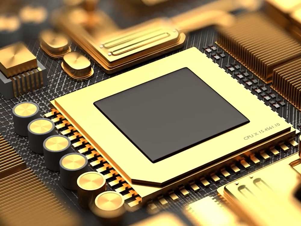
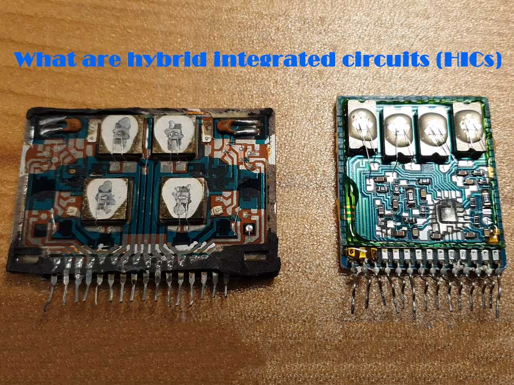
Hybrid integrated circuits (HICs) integrate a variety of electronic components on a substrate to form a complete circuit function.

What is the definition of hybrid integrated circuits (HICs)

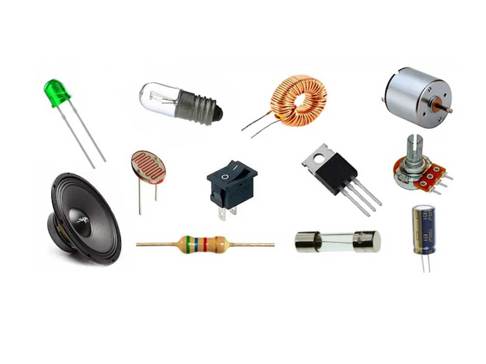
Hybrid integrated circuits (HICs) are organic wholes composed of multiple electronic components (active and passive devices) integrated onto the same semiconductor wafer through different processes.

It has the characteristics of miniaturization, lightweight, and high reliability, and is widely used in military, aerospace, electronics and other fields.

Hybrid Integrated Circuit Fabrication – Monolithic Microwave Integrated Circuits

What are the disadvantages of hybrid integrated circuits (HICs)

The disadvantages of hybrid integrated circuits mainly include the following aspects:

  1. Higher cost: The manufacturing of hybrid integrated circuits requires precise control of the size, location and connection methods of each component, so the manufacturing cost is high. At the same time, because it requires multiple independent components to be assembled together, the assembly cost is also high.
  2. Reliability issues: The components in hybrid integrated circuits are combined together through physical or chemical connections, so reliability issues at the connection points may affect the performance and reliability of the entire circuit.
  3. Difficulty in maintenance: Since the components in hybrid integrated circuits are closely arranged, it is difficult to replace or repair faulty components.

What are the advantages of hybrid integrated circuits (HICs)

What are the advantages of hybrid integrated circuits hics give? Hybrid integrated circuits (HICs) are microcircuits that integrate multiple electronic components on a single substrate. Its advantages mainly include:

  1. High assembly density: Hybrid integrated circuits can integrate multiple components in a limited space, thereby increasing the assembly density of the circuit, reducing the volume and weight of the product, and helping to achieve miniaturization and miniaturization of electronic equipment.
  2. High reliability: Because the components in hybrid integrated circuits are integrated together rather than connected through external connectors, there are fewer connection points and the risk of failure due to poor connections is reduced. At the same time, the components integrated together are not easily affected by the external environment, further improving the reliability of the circuit.
  3. Good electrical properties: The components in hybrid integrated circuits are made through thin film technology and have good electrical properties, such as low resistance, low capacitance, etc. This results in a circuit with lower signal loss and noise interference, improving circuit performance.
  4. Flexible design: Hybrid integrated circuits can be customized according to different application requirements using different materials and processes. This gives designers the flexibility to select components, materials and processes based on specific needs to achieve optimal performance and reliability.
  5. Easy to manufacture and maintain: The manufacturing process of hybrid integrated circuits is relatively simple, and standardization and mass production can be used to reduce production costs. At the same time, the maintenance of hybrid integrated circuits is relatively convenient. Only the entire circuit needs to be tested and repaired, and there is no need to inspect each component one by one.

Hybrid integrated circuits (HICs) have obvious advantages in miniaturization, reliability, electrical performance, design flexibility, and manufacturing maintenance, and are widely used in communications, computers, medical, aerospace and other fields.

What are hybrid integrated circuits examples

Hybrid circuits and integrated circuits through the microscope

A very close look at two hybrid amplifier circuits: An STK type from the late 70s and an SVI 3102 from the late 80s which also includes some exposed integrated circuits. This video explains what hybrid circuits are and how they are different from integrated circuits.

What does Hybrid Integrated Circuits (HICs) SIP mean

SIP (System In a Package) is a system that prioritizes the assembly of multiple active electronic components with different functions, optional passive components, and other components such as MEMS or optical components to achieve certain functions. A single standard package forms a system or subsystem.

What does Hybrid Integrated Circuits (HICs) SIP mean

SIP integrates multiple functional chips, including processors, memories and other functional chips, into one package to achieve a basically complete function. Architecturally speaking, SIP integrates multiple active electronic components with different functions and optional passive devices into one package to achieve a basically complete function.

SIP uses different chips to be packaged side by side or superimposed, corresponding to SOC (system on chip). The difference is that system-level packaging uses different chips to be packaged side by side or stacked, while SOC is a highly integrated chip product.

In addition, the advantages of SIP include good signal integrity, lower power consumption, and smaller size, making it an efficient and reliable packaging solution that is widely used in various fields, such as communications, computers, etc. , consumer electronics, etc.

What does Hybrid Integrated Circuits (HICs) SOP mean

SOP (Small Out-Line Package) is a common form of component packaging, mainly used in the packaging of integrated circuits. Its pins are led out from both sides of the package in a gull-wing shape (L-shape) and are suitable for surface mount technology (SMT).

SOP packaging has a wide range of applications and can be used in memory LSI, microcomputer circuits and other fields. In areas where the number of pins does not exceed 40, SOP is the most popular surface mount package. The typical pin center distance is 1.27mm (50mil), and others are 0.65mm and 0.5mm. SOP with an assembly height of less than 1.27mm is also called TSOP (Thin SOP).

With the continuous advancement of technology and changing application requirements, the application of SOP packaging has gradually decreased. Now, smaller and more compact packaging forms such as QFP (Quad Flat Package), BGA (Ball Grid Array), etc. have become mainstream.
SOP packaging is a simple, reliable and economical packaging form, mainly suitable for packaging of small and medium-sized integrated circuits.

What does hybrid integrated circuits (HICs) DIP mean

Hybrid integrated circuit DIP (Dual In-line Package) is a type of packaging for electronic components, mainly used for packaging integrated circuits. This package has two rows of equidistant pins, each row of pins are arranged opposite each other, and the spacing between each pin is the same.

In hybrid integrated circuits, DIP packaging is the most common form of packaging, with the number of pins generally not exceeding 100. It is mainly used to insert into a socket or socket on a printed circuit board (PCB) to facilitate connection with a plug or socket. A DIP packaged integrated circuit has two rows of equidistant pins formed along both sides of the package for connection to a plug or socket.

DIP packaging has many advantages, such as its simple packaging structure, high reliability, and strong scalability. Due to its small number of pins, it is very suitable for packaging of small and medium-sized integrated circuits. In addition, the price of DIP packaging is relatively close to the people, which helps reduce production costs.

However, with the development of technology and changing packaging requirements, the application of DIP packaging has gradually decreased. Now, smaller and more compact packaging forms such as QFP (Quad Flat Package), BGA (Ball Grid Array), etc. have become mainstream.

Hybrid integrated circuit DIP is a simple, reliable and economical packaging form, which is mainly suitable for the packaging of small and medium-sized integrated circuits.

What are the packaging methods of hybrid integrated circuits (HICs)

Hybrid integrated circuit is a circuit design method that integrates multiple functional modules into a single chip. The following is a detailed introduction to common hybrid integrated circuit packaging methods:

Dual in-line package (DIP)

This is a traditional package with two pins arranged in parallel. It is suitable for larger chip sizes and is usually manually inserted into a socket. However, due to its relatively large size, it is no longer commonly used.

Small Outline Integrated Circuit (SOIC)

This is a common surface mount packaging method. It has two parallel-arranged straight-in pins, but is smaller and more compact. SOIC packages are widely used in various applications, especially in consumer electronic devices.

Quad Flat Package (QFP)

This is a surface mount package with four neatly arranged pins. It was more common in early chip packaging and was suitable for larger size and higher pin count chips.

Ball Grid Array (BGA)

BGA is a surface mount package with pins arranged in the form of balls on the bottom. These balls are used to connect to pads on a printed circuit board (PCB). Due to the higher pin count, BGA packages can provide better electrical performance and thermal performance.

Land Grid Array (LGA)

LGA is a surface mount package in which the pins are arranged on the bottom in the form of metal pillars through holes instead of pads. This packaging method makes it easier for the pins to connect to the PCB, while providing better electrical performance and heat dissipation performance.

Chip-scale package (CSP)

CSP is a very small package usually used in combination with Ball Grid Array (BGA) or Land Grid Array (LGA). It has very high pin density and compact size, making it suitable for applications requiring a high degree of integration and miniaturization.

These packaging methods are only part of hybrid integrated circuit packaging. There are other special types of packaging methods, such as Quad Flat No Leads (QFN), Thin Small Outline Package (TSOP), etc. Based on specific application needs, design engineers can select the appropriate packaging method to meet functional requirements, space constraints and manufacturing requirements.

Difference analysis between DIP, SOT, SIP and SOP

The following is an analysis of the differences between DIP, SOT, SIP and SOP:

  • DIP: Dual in-line package. The pins are drawn from both sides of the package. The packaging materials are plastic and ceramic. DIP is the most popular plug-in package, and its application range includes standard logic IC, memory LSI, microcomputer circuits, etc.
  • SOP: One of the surface mount packages, the pins are led out from both sides of the package in a seagull wing shape (L shape). SOP packaging has a wide range of applications. In addition to being used in memory LSI, it is also used in fields with no more than 10 to 40 input and output terminals. SOP is the most widely used surface mount package.
  • SIP: System-level packaging, which assembles multiple active electronic components with different functions, optional passive components, and other components such as MEMS or optical components together to form a single standard package that achieves certain functions. A system or subsystem.

In addition, SOT (Surface Mounted Package) is another surface mount package form, with pins leading out from both sides or one side of the package in a round, flat shape, etc. Compared with DIP, SOP and SIP, SOT is smaller in size and suitable for miniaturized electronic products.

In general, these four packaging forms have their own characteristics, and the choice of which packaging form depends on the specific application needs and product requirements.

About Hybrid Integrated Circuits (HICs): Principles, Technologies and Applications

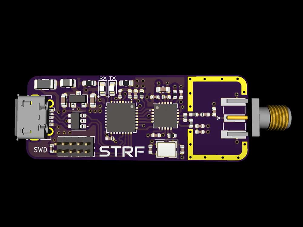
Hybrid Integrated Circuits (HICs for short) is a circuit system that integrates multiple electronic components on a substrate and combines them through physical, chemical or mechanical connections to achieve specific functions.

Compared with traditional integrated circuits, hybrid integrated circuits have higher flexibility, scalability and reliability, so they have been widely used in many fields.

Let’s continue to introduce the principles, technologies and applications of hybrid integrated circuits.

Principles of Hybrid Integrated Circuits (HICs)

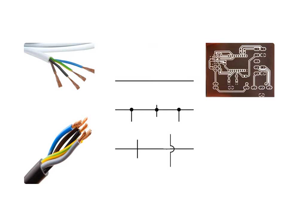
The core of hybrid integrated circuits is to integrate different electronic components on the same substrate and realize specific circuit functions through interconnection. These components can be manufactured independently, such as semiconductor chips, resistors, capacitors, etc., or they can be processed directly on the substrate. In a hybrid integrated circuit, components are connected through conductive materials to form a complete circuit system.

The design and manufacturing of hybrid integrated circuits involves knowledge from multiple disciplines, including electronic engineering, materials science, mechanical engineering, etc. In the design, factors such as circuit performance, reliability, power consumption, and manufacturing cost need to be comprehensively considered. During the manufacturing process, the size, location, and connection of each component need to be precisely controlled to ensure the reliability and performance of the circuit.

Hybrid Integrated Circuits (HICs) Technology

  1. Substrate selection and processing: The substrate is the basis of hybrid integrated circuits, and its selection has an important impact on the performance and reliability of the circuit. Commonly used substrate materials include ceramics, silicon, glass, etc., which need to be selected according to circuit requirements. Substrate processing includes steps such as cleaning, drying, and metallization, and is an important step in the manufacturing process.
  2. Component manufacturing and assembly: The components in hybrid integrated circuits can be independent or directly processed on the substrate. The manufacturing of components involves a variety of technologies, such as thin film deposition, photolithography, etching, etc. Assembly is the process of placing each component on the substrate according to the design requirements and completing the connection. The accuracy and reliability of assembly have a significant impact on the performance and reliability of the circuit.
  3. Circuit interconnection and packaging: Each component in a hybrid integrated circuit needs to be connected to each other to form a complete circuit system. Circuit interconnection involves the selection and processing of conductive materials, such as metal wires, solder, etc. Packaging is to protect and seal the completed hybrid integrated circuit to prevent the impact of the external environment on the circuit, while protecting the internal components from damage.
  4. Testing and Reliability Verification: After manufacturing is completed, the hybrid integrated circuit needs to be tested and reliability verified to ensure that its performance and reliability meet the design requirements. Test content includes functional testing, performance testing, environmental adaptability testing, etc. Reliability verification can be carried out through accelerated aging tests and other methods.

What are hybrid integrated circuits used for

Hybrid integrated circuits have been widely used in many fields due to their flexibility and high reliability. Here are some common application areas:

  1. Aerospace and Avionics: Hybrid integrated circuits are widely used in the aerospace and aviation fields. Due to their high reliability and stability, they are suitable for harsh environmental conditions. For example, the control systems and navigation systems of aircraft and satellites all use hybrid integrated circuits in large quantities.
  2. Automotive Electronics: In the field of automotive electronics, hybrid integrated circuits are also widely used. For example, automobile engine control systems, ABS anti-lock braking systems, etc. all use hybrid integrated circuits to implement complex functions.
  3. Industrial Control and Automation: In the field of industrial control and automation, hybrid integrated circuits are used to implement various control and monitoring functions. For example, industrial robots, automated production lines, etc. all use hybrid integrated circuits.
  4. Medical Devices: In the field of medical devices, hybrid integrated circuits are widely used due to high requirements for reliability and safety. For example, pacemakers, medical sensors, etc. all use hybrid integrated circuits to implement complex functions.
  5. Communication and network equipment: In the field of communication and network equipment, hybrid integrated circuits are used to implement various signal processing and transmission functions. For example, mobile phones, routers, switches, etc. all use hybrid integrated circuits to achieve high-speed data transmission and signal processing.

Future development trends and challenges

With the continuous development of science and technology, the technology and applications of hybrid integrated circuits are also constantly improving. In the future, the development of hybrid integrated circuits will mainly focus on the following aspects:

  1. High performance and high reliability: With the continuous expansion of applications and the continuous improvement of demands, the requirements for the performance and reliability of hybrid integrated circuits are becoming higher and higher. The future will require the development of more advanced manufacturing and materials technologies to improve circuit performance and reliability.
  2. Integration and miniaturization: Integration and miniaturization are important trends in the future development of hybrid integrated circuits. By continuously increasing the level of integration and reducing the size of components, circuit volume can be reduced and performance improved. At the same time, miniaturization also helps improve circuit reliability and reduce manufacturing costs.
  3. Intelligence and automation: Intelligence and automation are also important development directions for hybrid integrated circuits in the future. By introducing artificial intelligence and automation technology, intelligent circuit design and manufacturing processes can be realized, improving production efficiency and product quality.
  4. Environmental protection and sustainable development: With the increasing emphasis on environmental protection issues, the development of environmentally friendly hybrid integrated circuit manufacturing technology is also an important trend in the future. By using environmentally friendly materials and processes.

What does DRV2605YZFR mean?

What does DRV2605YZFR mean?

DRV2605YZFR has multiple meanings. If you think about it from the perspective of electrical products, it may be a semiconductor PMIC power management chip produced by Texas Instruments (TI).

DRV2605YZFR YouTube video explanation

DRV2605 ERM/LRA Haptics Driver Overview – Mark demonstrates the DRV2605 ERM/LRA haptics driver – TI’s new, one-of-a-kind solution that simplifies system design in the fast-growing area of haptics user interface.

It has the functions of a voltage regulator and a voltage controller and can be used for battery management.

On the other hand, coming from the engineering world, it is an ERM/LRA haptic driver with waveform libraries and automatic resonance tracking.

What are the advantages and disadvantages of DRV2605YZFR?

HAPTIC – Example

The DRV2605YZFR is a low-voltage haptic driver that includes a library of haptic effects and provides a high-quality closed-loop actuator control system.

This architecture helps improve actuator performance, speeding up coherence, start-up and braking times, and can provide input signals via a shared I2C-compatible bus or PWM.

The DRV2605YZFR’s smart loop architecture device allows simple automatic resonant driving of the LRA as well as feedback-optimized ERM driving, allowing automatic overspeeding and braking.

In addition, it has a functional system that automatically transitions to open loop if the LRA actuator does not generate a valid back-EMF voltage.

When valid back EMF voltage is detected, the DRV2605YZFR device automatically synchronizes with the LRA.
As for its specific advantages and disadvantages, it needs to be evaluated based on specific application scenarios and needs.

What does DRV2605YZFR mean?

DRV2605YZFR tactile driver price

What is the price of DRV2605YZFR tactile driver in China? What is the price of DRV2605YZFR?

Specific prices for DRV2605YZFR vary by supplier and stock type.

According to the price information provided by a merchant, the price of DRV2605YZFR is 6.9156 yuan including tax for 1 piece, and 5.4782 yuan for 30 pieces. These prices are for reference only.

How much does the DRV2605YZFR haptic driver cost in the US?

The price of the DRV2605YZFR haptic driver varies depending on market supply and demand and various sales channels. Here are some possible reference price ranges:

The price of the DRV2605YZFR is around $10 to $15 on some online electronic parts distributor websites.
Some professional electronic parts suppliers and distributors may sell this product at wholesale prices, which may be in the lower range, such as around $8 to $12.

What is the price of DRV2605YZFR haptic driver in India?

The price of the DRV2605YZFR haptic driver in India will also vary depending on market supply and demand and various sales channels. Here are some possible reference price ranges:

The price of DRV2605YZFR is around Rs 500 to Rs 800 on some online electronic parts distributor websites.
Some professional electronic parts suppliers and distributors may sell the product at wholesale price, which may be in a lower range, say around Rs 400 to Rs 600.

Note that when purchasing electronic components, if you purchase large quantities and establish long-term cooperative relationships with suppliers, you may get more competitive prices.

It should be noted that these prices are for reference only and actual prices may vary depending on suppliers, purchase quantities, currency exchange rates and other factors.

It is recommended to contact the relevant supplier before purchasing to obtain the most accurate price information.

What are the application scenarios of DRV2605YZFR?

The application scenarios of DRV2605YZFR may include but are not limited to the following aspects:

  1. Tactile feedback: DRV2605YZFR, as a tactile driver, can be used to produce tactile feedback effects. In the fields of virtual reality, games, robots, etc., the DRV2605YZFR drives the actuator to generate vibration or touch, providing users with tactile feedback and enhancing immersion and interactive experience.
  2. Motion control: DRV2605YZFR can be used to control the movement of electric actuators, such as motors, servo systems, etc. Through the drive and control functions of DRV2605YZFR, precise motion control can be achieved, such as position, speed and acceleration adjustment, which is widely used in robots, automation equipment and other fields.
  3. Vibration suppression: DRV2605YZFR can be used to suppress vibration of equipment. By adjusting the driving parameters of DRV2605YZFR, the vibration frequency and amplitude of the actuator can be effectively controlled, reducing the vibration and noise generated by the equipment during operation.
  4. Energy harvesting: DRV2605YZFR can be used in the field of energy harvesting to provide energy supply for equipment by collecting vibration energy in the environment and converting it into electrical energy. This application method helps realize self-powered equipment and systems and reduces dependence on traditional energy sources.

It should be noted that the above application scenarios are only possible examples, and specific applications depend on actual needs and scenarios.

Summary about DRV2605YZFR

The DRV2605YZFR is a haptic driver with waveform library and automatic resonance tracking designed for ERM (eccentric rotating mass) and LRA (linear resonance actuator). It features an advanced smart loop architecture that helps improve actuator performance, including acceleration consistency, start-up time and braking time. At the same time, it provides a shared I2C compatible bus or PWM input signal interface to facilitate integration with other systems.

In addition, DRV2605YZFR also has automatic resonance driving and feedback optimization functions, which can realize simple driving of LRA actuators and optimized control of ERM actuators. It also supports automatic overspeed and braking functions to ensure system stability and safety.

In terms of software, DRV2605YZFR is compatible with Immersion’s TouchSense software library, which contains a wealth of predefined waveforms and effects, making it easy to implement various tactile feedback effects. At the same time, it also supports real-time playback mode, allowing the host processor to play custom waveforms directly.

Overall, the DRV2605YZFR is a powerful, easy-to-integrate tactile driver suitable for various application scenarios that require tactile feedback. Its intelligent loop architecture and optimized control algorithm ensure the high performance and consistency of the actuator, providing users with an excellent tactile experience.

What systems does DRV2605YZFR support?

DRV2605YZFR is a tactile driver whose core function is to generate tactile feedback effects. It can be integrated with a variety of systems to implement tactile feedback functionality. For example, it can be integrated with mobile devices such as game controllers or mobile phones to provide immersive tactile feedback effects and enhance the user’s interactive experience. In addition, DRV2605YZFR can also be integrated with virtual reality (VR) and augmented reality (AR) systems to provide users with a more realistic virtual environment interactive experience.
It should be noted that which systems are specifically supported need to be evaluated based on actual application scenarios and needs.

What documents are required for the import of electronic components?

What documents are required for the import of electronic components?

Electronic component import certificates refer to a series of certification documents that need to be processed in accordance with national laws, regulations and relevant policy requirements when importing electronic components, including import licenses, automatic import licenses, 3C certifications, etc., to prove the authenticity of the goods. Legality, safety and compliance with quality standards.

Detailed introduction to the documents and procedures required for the import of electronic components

Walking Through a Big Electronic Component Market in China – For everyone designing electronic circuits. I recorded this when visiting Shenzhen.

As the basic component of modern electronic equipment, the import business of electronic components occupies an important position in global trade. Due to the wide variety of electronic components, their high technical content, and the involvement of national security, environmental protection, quality and other factors, a series of documents and procedures are required when importing. The following will provide a detailed introduction to the documents and procedures required for the import of electronic components.

Documents required for import

Import license

According to relevant national laws and regulations, some electronic components are restricted import commodities and require advance application for an import license from relevant national departments. When applying for an import license, you need to provide the importer’s basic information, imported commodity list, technical specifications, usage description and other materials. Import operations can only be carried out after obtaining the import license.

Automatic import license

For some electronic components, such as sensitive products involving national security, environmental protection and other factors, you need to apply for an automatic import license.

The application process for an automatic import license is similar to that of an import license, but the approval process is more stringent. Import operations can only be carried out after obtaining an automatic import license.

3C certification

3C certification is the abbreviation of China Compulsory Product Certification. It is a compulsory product certification system implemented for some products involving personal safety, animal and plant life safety, environmental protection and national security. Some electronic components such as power adapters, switching power supplies, etc. require 3C certification. When applying for a 3C certification, you need to provide product technical specifications, test reports, manufacturer information and other materials. After obtaining the 3C certification, import and sales can be carried out.

Certificate of origin

Certificate of origin is an official document proving the origin of goods, usually issued by the government of the exporting country or relevant agencies. When importing electronic components, you need to provide a certificate of origin to prove the source of the goods and enjoy relevant tariff preferential treatment. The process for applying for a certificate of origin varies from country to country and region. Generally, you need to provide the exporter’s basic information, product list, production process and other materials.

Packing list, invoice and contract

Packing list, invoice and contract are the basic documents for imported electronic components. The packing list details the product name, specifications, quantity, weight and other information of each box of goods; the invoice lists the price, total amount and other information of the goods; the contract stipulates the rights and obligations of the buyer and seller. These documents are essential when going through import customs declaration procedures.

Import process of electronic components in China

Sign foreign trade contracts with foreign suppliers

Before importing electronic components, you first need to sign a foreign trade contract with a foreign supplier. The contract should clearly stipulate the product name, specifications, quantity, price, delivery period and other terms of the goods. At the same time, both parties should reach an agreement on payment methods, transportation methods, etc. Signing a foreign trade contract is the first step to import electronic components, and it is also an important measure to protect the rights and interests of both parties.

Apply for import license and automatic import license (if necessary)

According to relevant national laws and regulations, some electronic components require an import license or automatic import license. After signing a foreign trade contract, you should promptly apply for relevant certificates from the relevant national departments. After obtaining the certificate, subsequent operations can be carried out.

Apply for 3C certification (if necessary)

For some electronic component products involving personal safety, animal and plant life safety, environmental protection and national security, 3C certification is required. When applying for a 3C certification certificate, the application and testing should be carried out in accordance with relevant national standards and procedures. After obtaining the 3C certification, import and sales can be carried out.

Prepare documents such as packing list, invoice and contract

Before the goods are shipped, documents such as packing lists, invoices and contracts should be prepared. These documents should detail the product name, specifications, quantity, price and other information of the goods, and comply with international trade practices and relevant national regulations. Only after the documents are ready can subsequent operations be carried out.

Arrange transportation and insurance matters

According to the provisions of the foreign trade contract and the actual situation, select the appropriate transportation method and insurance company for cargo transportation and insurance. The mode of transportation can be sea transportation, air transportation or land transportation; insurance companies should choose insurance companies with good reputation and high quality services for insurance. Ensuring the safety and security of goods during transportation is one of the important aspects of importing electronic components.

Complete import declaration procedures

After the goods arrive at the destination port, they should be declared to the customs in time and go through the import declaration procedures. When going through customs declaration procedures, complete documentation should be provided and duties and other taxes should be paid in accordance with regulations. The goods can be released for pickup only after the customs has inspected and reviewed the goods. It should be noted that some electronic components may require statutory inspection or commodity inspection before being released for delivery. Therefore, you should understand the relevant regulations and requirements and make preparations in advance before going through customs declaration procedures.

Arrange domestic transportation and warehousing matters

Detailed introduction to the documents and procedures required for the import of electronic components

After the goods are released for pickup, domestic transportation and warehousing matters should be arranged in a timely manner to transport the goods to the destination and properly kept to ensure the safety and integrity of the goods during transportation and to facilitate subsequent sales and use.

When arranging domestic transportation and warehousing matters Factors such as the characteristics, quantity, and transportation distance of the goods should be taken into consideration and appropriate transportation methods and warehousing facilities should be selected to reduce costs and improve efficiency to ensure that the entire import process proceeds smoothly and achieves the desired results.

The above content introduces in detail the documents and overall procedures required for the import of electronic components. In actual operations, enterprises should fully understand the relevant policies and regulatory requirements and actively cooperate with government departments to ensure the smooth progress of the business and also strengthen their own awareness of compliance. and risk management capabilities to avoid losses and risks resulting from regulatory violations.

What are the Korean semiconductor companies in China?

Top 7 Korean semiconductor companies in China

South Korea is an important semiconductor industry country in the world. It has a complete semiconductor industry chain and advanced technology, and it occupies an important position in the global semiconductor market.

In recent years, Korean semiconductor companies have actively expanded into the Chinese market and invested and built factories in China, making positive contributions to the development of China’s semiconductor industry.

Market distribution of Korean semiconductor companies in China

Currently, Korean semiconductor companies in China are mainly distributed in the following fields:

Memory chips: Korean companies such as Samsung Electronics, SK Hynix, and Micron Technology have established memory chip production bases in China, mainly producing DRAM and NAND flash memory chips.

Logic chips: Samsung Electronics, SK Hynix, Intel and other Korean companies have established logic chip production bases in China, mainly producing central processing units (CPUs), graphics processing units (GPUs) and other chips.

Market distribution of Korean semiconductor companies in China

Analog chips: Korean companies such as Samsung Electronics, LG Semiconductor, and Maxim have established analog chip production bases in China, mainly producing analog circuit chips.

Power devices: Korean companies such as Samsung Electronics, LG Semiconductor, and NXP have established power device production bases in China, mainly producing power semiconductor devices.

Packaging and testing: Korean companies such as Samsung Electronics, SK Hynix, and ASE have established packaging and testing factories in China, which mainly provide packaging and testing services for the chips they produce.

As industry works to restore the global supply of semiconductors, South Korea is working to position itself at the center of the new supply chain that emerges on the other side of the shortage.

It’s working to build its own infrastructure for the entire chipmaking process, which will drastically reduce its reliance on foreign sourcing. Kim Sung-min reports.

Semiconductor factory laboratory in South Korea

Aiming to cement South Korea’s dominant position in the global semiconductors supply chain,… the government on Thursday unveiled its so-called “K-Semiconductor Belt Strategy”. The strategy will see a large scale investment from private firms with tax breaks and financial and infrastructure support coming from the government. “Our country’s semiconductor firms will create the world’s biggest chip supply chain in South Korea over the next ten years through injecting more than 451 billion U.S. dollars. In return, the government has come up with a large scale support package.” Among those firms, Samsung Electronics intends to invest more than 151 billion U.S. dollars in system semiconductors, and SK hynix will also expand its investment.

S. Korea to build world-leading semiconductor supply chain by 2030

Key to the plan is a semiconductor cluster… connecting three strips of facilities across the country to create a K-shape. The belt will encompass foundry manufacturing, materials and components production, as well as fabless manufacturing and packaging,…reducing the country’s dependency in all areas of the production process. Another pillar of the strategy is to drastically expand investment and tax incentives for the semiconductor sector.

Products from electronic component manufacturers and distributors

That includes tax breaks of up to 50 percent for research and development and 20 percent for facility investment for both SMEs and conglomerates. For facility investment,… around 9-hundred million U.S. dollars has been set aside for prime-rate loans. 10 years’ worth of water used at Yongin and Pyeongtaek,… within the chip cluster,… has been secured and the government aims to shoulder half the cost of the electricity used at the facilities.

K-Semiconductor Belt Strategy

The plan also includes training around 36-thousand more skilled personnel in the chip industry over the next ten years by expanding the related university and masters courses and class quotas. Coming up with a long term roadmap for strengthening the supply of automotive chips is also part of the plan.

Through the “K-Semiconductor Belt Strategy”, the country is aiming to double chip exports within ten years. It is also expected to create around 100-thousand new jobs in the country. Kim Sung-min, Arirang News.

Top 7 Korean semiconductor companies in China

Top 7 Korean semiconductor companies in China

The following is a detailed introduction to the major Korean semiconductor companies in China:

Samsung Electronics

The continuous development of semiconductors has changed the way we live today.
How are they made? What will these small ‘seeds’ grow into in the hyper-connected society?

What is a semiconductor?

Samsung Electronics is the world’s largest semiconductor company, and its semiconductor business covers memory chips, logic chips, analog chips, power devices and other fields.

Samsung Electronics has built multiple semiconductor production bases in China, mainly located in Suzhou, Nanjing, Wuxi, Jiangsu Province, and Chengdu, Sichuan Province.

The semiconductor products produced by Samsung Electronics in China are mainly sold to the domestic market and also exported to other regions around the world.

SK hynix

[Official] SK hynix PR Video (English Ver.)

SK Hynix is the world’s second largest memory chip company, and its main products are DRAM and NAND flash memory chips.

SK Hynix has built multiple semiconductor production bases in China, mainly located in Suzhou and Wuxi, Jiangsu Province, and Chengdu, Sichuan Province.

The semiconductor products produced by SK Hynix in China are mainly sold to the domestic market and also exported to other regions around the world.

Micron Technology

Micron Technology is the third largest memory chip company in the world, and its main products are DRAM and NAND flash memory chips.

Micron Technology has built multiple semiconductor production bases in China, mainly located in Chengdu. The semiconductor products produced by Micron Technology in China are mainly sold to the global market.

Intel

Intel semiconductor – Working In The Clean Room Inside The Fab | Intel

Intel is the world’s largest logic chip company, and its main products are central processing units (CPUs), graphics processing units (GPUs) and other chips. Intel has built multiple semiconductor production bases in China, mainly located in Beijing, Shanghai, and Chengdu. The semiconductor products produced by Intel in China are mainly sold to the global market.

LG Semiconductor

Korea’s LG Chem and U.S. auto giant GM to build US$ 2.3 bil. EV battery factory in Ohio

LG Semiconductor is the world’s leading analog chip company, and its main products are analog circuit chips. LG Semiconductor has built multiple semiconductor production bases in China, mainly located in Suzhou and Wuxi, Jiangsu Province. The semiconductor products produced by LG Semiconductor in China are mainly sold to the global market.

Maxim Integrated Products

Extend Battery Life in Space-Constrained Applications with ADI’s nanoPower Modules

Maxim is the world’s leading power device company, and its main products are power semiconductor devices. Maxim has built multiple semiconductor production bases in China, mainly located in Suzhou and Wuxi, Jiangsu Province. The semiconductor products produced by Maxim in China are mainly sold to the global market.

ADVANCED SEMICONDUCTOR ENGINEERING INC.

ASE is the world’s leading packaging and testing company, and its main business is to provide packaging and testing services to semiconductor companies.

ASE has multiple packaging and testing plants in China, mainly located in Suzhou and Wuxi, Jiangsu Province, and Shenzhen, Guangdong Province. ASE provides packaging and testing services to Huawei and many Korean semiconductor companies.

In recent years, with the development of China’s semiconductor industry, Korean semiconductor companies have continued to increase their investment in China.

It is expected that China will become an important market for Korean semiconductor companies in the future.

What are the semiconductor chip packaging materials?

What are the semiconductor chip packaging materials?

Semiconductor chip packaging materials refer to materials used for semiconductor chip packaging. Its main function is to protect the chip from erosion by the external environment and provide support, heat conduction, insulation and other functions for the chip.

There are many types of semiconductor chip packaging materials. According to their main materials, they can be divided into metal materials, plastic materials, ceramic materials, glass materials, etc.

Metallic material

Metal materials have good thermal conductivity, strength and corrosion resistance, and are a common choice for semiconductor chip packaging materials. Commonly used metal packaging materials include aluminum, copper, silver, gold, etc.

Aluminum

Aluminum is a lightweight, highly thermally conductive metal that is cost-effective and is the preferred packaging material for semiconductor chips. Aluminum packaging materials are mainly used for low-power, small, and thin chip packaging.

What are the semiconductor chip packaging materials?

Aluminum as a semiconductor packaging material has the following advantages:

  • It is light in weight and has a density of 2.7g/cm3, which is only 1/3 of copper, which helps reduce the weight and volume of the chip.
  • It has good thermal conductivity, with a thermal conductivity of 200W/(m·K), second only to silver and 2/3 of copper.
  • Low cost, the price is only 1/5 of copper.

Aluminum as a semiconductor packaging material also has the following disadvantages:

  • Low strength, the tensile strength is 90MPa, which is only 1/4 of copper.
  • It has poor corrosion resistance and is easily corroded by acids, alkalis, etc.

Copper ( Cuprum )

Copper has higher thermal conductivity and strength, but also costs more. Copper packaging materials are mainly used for high-power and high-power chip packaging.

Copper has the following advantages as a semiconductor packaging material:

  • It has good thermal conductivity and the thermal conductivity is 400W/(m·K), which is twice that of aluminum.
  • High strength, the tensile strength is 200MPa, which is 2.2 times that of aluminum.
  • It has good corrosion resistance and can resist acid, alkali and other corrosion.

Copper as a semiconductor packaging material also has the following disadvantages:

  • It is heavier and has a density of 8.9g/cm3, which is 3 times that of aluminum.
  • The cost is high, the price is only 2 times that of aluminum.

Silver ( Argentum )

How to Write the Electron Configuration for Ag and Ag+ Introduction to the chemical properties of silver ions and silver atoms

Silver has the highest thermal conductivity, but is also the most expensive. Silver packaging materials are mainly used for chip packaging that require extremely high thermal conductivity, such as power amplifiers, radio frequency chips, etc.

Silver has the following advantages as a semiconductor packaging material:

  • It has good thermal conductivity, with a thermal conductivity coefficient of 430W/(m·K), which is 1.07 times that of copper.
  • High conductivity, 63.5S/m, 1.62 times that of copper.
  • High gloss and good decorative properties.

Silver also has the following disadvantages as a semiconductor packaging material:

  • It is heavier and has a density of 10.5g/cm3, which is 4 times that of aluminum.
  • The cost is high, the price is only 10 times that of aluminum.

Gold ( Aurum )

Where the Chemical Symbol AU Comes From: Did You Know?

Many people know the chemical symbol for gold is “Au”, but not as many people know the origin of the term, or why the atomic number for gold is 79, or where the word gold comes from.

Gold has good electrical conductivity, corrosion resistance and aesthetics, and is mainly used for high-end, high-performance chip packaging.

Gold has the following advantages as a semiconductor packaging material:

  • It has good electrical conductivity, with a conductivity of 41.7S/m, which is 1.67 times that of copper.
  • It has good corrosion resistance and can resist acid, alkali and other corrosion.
  • It has good aesthetics and good decorative properties.

Gold also has the following disadvantages as a semiconductor packaging material:

  • The cost is high, the price is only 100 times that of aluminum. Gold is expensive due to its reserves and difficulty in mining, which increases the cost of semiconductor packaging.
  • Difficulty in processing: Gold has a high hardness, which makes it prone to wear and scratches during processing, resulting in a reduction in packaging yield.
  • Poor heat dissipation performance: Gold is a poor conductor with poor thermal conductivity, which is not conducive to heat dissipation of semiconductor devices.
  • Insufficient ductility: Gold is prone to deformation when subjected to high temperatures or external forces, affecting the accuracy and reliability of packaging.

Although gold has some shortcomings as a semiconductor packaging material, it still has irreplaceable advantages in some fields, such as high conductivity, high chemical stability and good corrosion resistance. In practical applications, appropriate packaging materials need to be selected according to specific needs to achieve optimal performance and cost-effectiveness.

Plastic material

What are Plastics? | Don’t Memorise

Plastic materials have good insulation, mechanical strength and processability and are another common choice for semiconductor chip packaging materials. Commonly used plastic packaging materials include epoxy resin, polyimide, polytetrafluoroethylene, etc.

Epoxy resin

Epoxy resin is a commonly used plastic packaging material with good insulation, mechanical strength and processability. Epoxy resin packaging materials are mainly used for low-power, small, and thin chip packaging.

Polyimide

Polyimide is a high-performance plastic packaging material with good heat resistance, corrosion resistance and high-frequency performance. Polyimide packaging materials are mainly used for high-power, high-frequency, and high-reliability chip packaging.

PTFE

PTFE is a plastic packaging material with good corrosion resistance, high temperature resistance and low friction. PTFE packaging materials are mainly used for chip packaging that require extremely high corrosion resistance and high temperature resistance, such as power amplifiers, radio frequency chips, etc.

Ceramic material

Ceramic materials have good heat resistance, corrosion resistance and mechanical strength, and are an important choice for semiconductor chip packaging materials. Commonly used ceramic packaging materials include alumina, silicon nitride, Si3N4, etc.

Alumina

Aluminum oxide is a commonly used ceramic packaging material with good heat resistance, corrosion resistance and mechanical strength. Alumina packaging materials are mainly used for high-power, high-frequency, and high-reliability chip packaging.

silicon nitride

Silicon nitride is a ceramic packaging material with higher heat resistance, corrosion resistance and mechanical strength. Silicon nitride packaging materials are mainly used for chip packaging that require extremely high heat resistance and corrosion resistance, such as power amplifiers, radio frequency chips, etc.

Si3N4

Si3N4 is a ceramic packaging material with good heat resistance, corrosion resistance and mechanical strength. Si3N4 packaging materials are mainly used for high-frequency, high-reliability chip packaging.

Glass material

Glass material has good heat resistance, corrosion resistance and light transmittance, and is a special choice for semiconductor chip packaging materials. Commonly used glass packaging materials include quartz glass, borosilicate glass, etc.

Quartz glass

Quartz glass is a glass packaging material with good heat resistance, corrosion resistance and light transmittance. Quartz glass packaging materials are mainly used for chip packaging that require extremely high heat resistance, corrosion resistance and light transmittance, such as optical chips, lasers, etc.

Borosilicate glass

Borosilicate glass is a glass with low thermal expansion coefficient, high heat resistance, high chemical stability and high optical transmittance. Its main components are silicon dioxide (SiO2), boron oxide (B2O3) and sodium oxide (Na2O). Among them, the content of boron oxide is between 6% and 15%, which is the main factor that determines the performance of borosilicate glass.
Low thermal expansion coefficient is one of the distinctive features of borosilicate glass. Its thermal expansion coefficient is about 1/3 of ordinary glass, so it has good thermal shock resistance and can withstand large temperature changes. This allows borosilicate glass to maintain its shape and properties at high temperatures, making it ideal for applications that need to withstand high temperatures, such as electric heaters, cookware, optical instruments, etc.
High heat resistance is another important feature of borosilicate glass. Its softening point temperature is about 1000°C, which is much higher than the softening point temperature of ordinary glass. Therefore, borosilicate glass can be used at high temperatures for a long time and has good corrosion resistance.
High chemical stability is one of the important properties of borosilicate glass. It has good corrosion resistance to chemicals such as acids, alkalis, and salts, so it can be used in various chemical environments.
High optical transmittance is another advantage of borosilicate glass. Its optical transmittance can reach over 90%, making it very suitable for optical applications.
Borosilicate glass has the above-mentioned excellent properties, so it has been widely used in semiconductor chip packaging. It is mainly used in the following areas:
High temperature packaging: Borosilicate glass has good heat resistance and can be used for high temperature packaging, such as power device packaging, LED packaging, etc.
Chemical packaging: Borosilicate glass has good chemical stability and can be used for chemical packaging, such as liquid crystal display packaging, optoelectronic device packaging, etc.
Optical packaging: Borosilicate glass has good optical transmittance and can be used for optical packaging, such as optical fiber packaging, laser packaging, etc.
In recent years, with the continuous development of semiconductor technology, the performance requirements for chip packaging materials have become increasingly higher. Borosilicate glass will continue to maintain its important position in the field of semiconductor chip packaging due to its excellent properties.

Detailed process of shipping electronic components from China to the United States

Detailed process of shipping electronic components from China to the United States

The global supply chain of electronic components is an important pillar of the modern electronics industry, and the trade of electronic components between China and the United States is a key part of this system.

For many businesses and individuals in the United States, understanding how to purchase and ship electronic components from China to the United States is an important business link.

This article will introduce this process in detail, including preparation, selection of transportation methods, logistics operations, customs clearance and delivery.

Preparation for transportation of electronic components

Determine the purchase list

First of all, it is necessary to clarify the specific model, specification and quantity of the electronic components to be purchased. This facilitates subsequent communication with suppliers, signing of contracts, and logistics arrangements.

Find suitable suppliers

Find reliable suppliers who can provide the products you need through electronic component trading platforms, industry exhibitions or directly contact electronic component manufacturers in China. When selecting a supplier, factors such as its reputation, product quality, price, and delivery capabilities need to be considered.

Sign the purchase contract

Sign a purchase contract with the selected supplier to clarify the rights and obligations of both parties, including key terms such as product specifications, quantity, price, payment method, and delivery time. In addition, the contract should also include important contents such as quality assurance, liability for breach of contract and methods of resolving disputes.

Select transportation method for electronic components

Choose the appropriate transportation method based on the characteristics, quantity and delivery time requirements of electronic components. Common shipping methods include air freight, sea freight and express delivery.

Air transport

Air transportation is fast and safe, and is suitable for small batches of high-value electronic components. However, air freight costs are relatively high and is suitable for goods with tight time requirements.

Air transport - Select transportation method for electronic components

Shipping

Sea transportation has low cost and large shipping volume, and is suitable for large quantities of low-value electronic components. However, sea transportation is slow and greatly affected by factors such as weather and port congestion.

Express delivery

The express delivery service is convenient and fast, and is suitable for small samples or emergency replenishment. However, express delivery costs are high and is not economical enough for large quantities of goods.

Logistics operations for electronic components

Packaging and labeling

Carry out reasonable packaging and marking according to the characteristics of electronic components and the requirements of the transportation method. Packaging should be strong enough to protect the goods from damage during transportation and comply with international transportation standards. At the same time, key information such as consignee information, cargo name, quantity, etc. should be clearly marked on the packaging for easy identification.

Logistics operations for electronic components

Book cabins/flights/express services

Book space (sea freight), flights (air freight) or express delivery services in advance according to the selected mode of transportation and the specific conditions of the goods. This helps ensure goods are shipped on time and reach their destination smoothly.

Bill of lading/air waybill/express bill processing

Before the goods are shipped, you need to confirm with the freight forwarder or logistics company that the information on the bill of lading (sea freight), air waybill (air freight) or courier note (express delivery) is accurate. These documents are important documents during the transportation of goods and need to be properly kept.

Electronic component procurement, export declaration and clearance procedures

  1. Export declaration procedures

Before the goods leave China, they need to be declared to the customs and go through export declaration procedures. This includes submitting necessary documents such as export declarations, commercial invoices, packing lists, etc., and paying the corresponding duties and fees (if applicable). After the customs declaration procedures are completed, the customs will release the goods and issue export certification documents.

  1. International transportation insurance arrangement (optional)

In order to reduce the risk during the transportation of goods, you can consider purchasing international transportation insurance. The insurance company will provide corresponding insurance plans based on the value of the goods and the mode of transportation. When purchasing insurance, you need to read the policy terms carefully and make sure you understand the coverage and disclaimers.

  1. Preparation for customs clearance procedures at destination and cooperation in completing customs clearance work (USA)

Before the goods arrive in the United States, you need to prepare the documents and information required for customs clearance in advance, and understand the U.S. import regulations and requirements. These documents usually include import licenses (if applicable), commercial invoices, packing lists, and other supporting documents required by customs (such as certificates of origin, etc.). At the same time, you need to cooperate with the consignee in the United States or its agent to complete customs clearance and pay the corresponding duties and fees (if applicable).

You may encounter various problems or delays during the customs clearance process, so you need to maintain timely communication with the consignee or agent in order to solve the problem in a timely manner and successfully complete the customs clearance work.
After customs clearance is completed, U.S. Customs will release the goods and deliver them to the consignee or its designated warehouse or location. At this point, the entire process of shipping electronic components from China to the United States is basically completed. The next step is the acceptance and payment of the consignee.

If everything goes well, the entire transaction process will be completed successfully. If problems arise, they need to be negotiated with the supplier or logistics company in time to avoid affecting subsequent cooperation. At the same time, it is also necessary to summarize and reflect on the entire transaction process in order to continuously improve and optimize the supply chain management process.

Precautions and suggestions for import and export of electronic components

There are many aspects that need to be paid attention to when importing and exporting electronic components. The following are some suggestions and precautions:

  1. Understand relevant regulations and standards: During the international procurement and transportation of electronic components, that is, before importing or exporting electronic components, you need to understand the laws, regulations and standards of the relevant countries and regions to ensure that the products comply with local requirements and standards. . For example, China has implemented the “Import and Export Commodity Inspection Law of the People’s Republic of China” and its implementation regulations, and implemented a compulsory product certification system for imported electronic components. They need to obtain the corresponding certification certificate and add a certification mark before they can be imported.
  2. Confirm product classification and regulatory requirements: There are many types of electronic components, and the regulatory requirements and import/export processes for different types of products may be different. Therefore, it is necessary to clarify the types of electronic components being imported or exported and understand the local regulatory requirements.
  3. Choose the appropriate logistics method: Choose the appropriate logistics method, such as sea transportation, air transportation, land transportation, etc., based on factors such as the type, quantity, volume, and weight of electronic components. For some high-value or high-risk electronic components, it is recommended to choose air transportation or specific sea transportation methods to ensure that the goods reach their destination safely and in a timely manner.
  4. Comply with customs declaration procedures and documentation requirements: When importing or exporting electronic components, you need to comply with local customs declaration procedures and documentation requirements. Documents that need to be provided include commercial invoices, packing lists, bills of lading, certificates of origin, quality certificates, etc. Ensure that the documents provided are true, accurate, complete and comply with local requirements and standards.
  5. Pay attention to tax and tariff issues: Different countries and regions may have different import tariffs and tax policies for electronic components, so you need to pay attention to tax and tariff issues when importing or exporting electronic components. Understand local tax policies and consult local customs or professionals in advance to avoid unnecessary losses.
  6. Strengthen quality control and safety testing: The quality and safety of electronic components are crucial to the overall performance and service life of the product. Therefore, when importing or exporting electronic components, it is necessary to strengthen quality control and safety testing to ensure that the products meet local quality requirements and safety standards.
  7. Establish a stable supply chain: It is crucial for an importer or exporter to establish a stable supply chain. Establish long-term cooperative relationships with reliable suppliers to ensure a stable, reliable and reasonably priced supply of electronic components. At the same time, understand the supplier’s quality assurance system and technical strength to ensure that the purchased electronic components have reliable quality assurance.
  8. Follow international trade rules and practices: International trade rules and practices are guidelines that importers or exporters must follow. Understand and follow the relevant rules of the World Trade Organization (WTO) and international practices such as the United Nations Convention on Contracts for International Trade and Sales to ensure the smooth development of trade. When trade disputes arise, you can seek legal assistance or consult professionals for advice to protect your own rights and interests.
  9. Strengthen market research and customer demand analysis: Before importing or exporting electronic components, it is necessary to conduct sufficient market research and customer demand analysis to understand the needs and trends of the local market. According to market demand and customer requirements, formulate targeted marketing strategies and product plans to improve the local competitiveness and market share of products.
  10. Maintain good communication with customers: During the process of importing or exporting electronic components, it is necessary to maintain good communication with customers and understand their specific needs and requirements. At the same time, we establish mutual trust relationships with customers, promptly resolve problems and disputes during the trade process, and improve customer satisfaction.

In short, the import and export of electronic components require attention to many issues and suggestions. Importers or exporters need to fully understand relevant regulations and standards, confirm product classification and regulatory requirements, choose appropriate logistics methods, comply with customs declaration procedures and document requirements, pay attention to tax and tariff issues, strengthen quality control and safety testing, and establish stable supply chain, comply with international trade rules and practices, strengthen market research and customer demand analysis, and maintain good communication with customers.

Following these recommendations will help you run a smooth import and export business of electronic components.

Research and analysis on the working principle of RF filter

Research and analysis on the working principle of RF filter

Radio frequency (RF) filters play a vital role in wireless communication systems. Their working principles are mainly based on the propagation characteristics of electromagnetic waves and the response characteristics of circuits.

This article will conduct an in-depth study and analysis of the working principle of RF filters, aiming to explore its performance characteristics and application scope.

Basic principles of RF filters

An RF filter is an electronic device used to filter a specific frequency range. The basic principle is to use the frequency response characteristics of the circuit to pass signals of specific frequencies through the filter while blocking signals of other frequencies. In wireless communication systems, RF filters are mainly used to filter, extract and suppress signals, thereby improving signal quality and stability.

Classification of RF filters

Research and analysis on the working principle of RF filter

According to different classification methods, RF filters can be divided into many types. According to the frequency response characteristics, it can be divided into low-pass filter, high-pass filter, band-pass filter and band-stop filter. According to the structural form, it can be divided into LC filters, crystal filters, ceramic filters and surface acoustic wave (SAW) filters. Each type of filter has different performance characteristics and application range.

Analysis of the working principle of RF filter

Basics of RF filters and different types of filters
  1. LC filter: The LC filter is composed of an inductor and a capacitor. By adjusting the values of the inductance and capacitance, the frequency response characteristics of the filter can be changed. When the inductor and capacitor meet certain conditions, the LC filter can achieve a band-pass or band-stop frequency response.
  2. Crystal filter: Crystal filter utilizes the piezoelectric effect of quartz crystal. By controlling the angle and vibration mode of crystal cutting, the required frequency response characteristics can be obtained. Crystal filters have high Q value and stability and are suitable for high-performance communication systems.
  3. Ceramic filter: Ceramic filter uses the dielectric constant and loss characteristics of ceramic materials. By controlling the shape and size of ceramic materials, the required frequency response characteristics can be obtained. Ceramic filters have the advantages of small size and low cost, and are widely used in fields such as mobile communications and satellite communications.
  4. SAW filter: SAW filter takes advantage of the propagation characteristics of sound waves on solid surfaces and can control sound waves by creating specific patterns on the surface of piezoelectric materials. SAW filters have the advantages of high Q value, low insertion loss and easy integration, and are widely used in the field of wireless communications.

RF filter performance parameters

  1. Cutoff frequency: refers to the frequency point at which the filter begins to suppress signals above or below a specific frequency.
  2. Bandwidth: refers to the frequency range of signals that the filter can pass.
  3. Insertion loss: refers to the degree of attenuation of the signal after the filter is connected to the circuit.
  4. Return loss: refers to the power loss caused by signal reflection.
  5. Q value: refers to the quality factor of the filter, which reflects the frequency selectivity and bandwidth of the filter.
https://www.youtube.com/watch?v=1sq8Cvju2Oo
Practical RF Filter Design and Construction

Application scenarios of RF filters

Practical RF Filter Design and Construction
  1. Mobile communications: Base stations and terminal equipment in mobile communications systems need to use high-performance RF filters to ensure signal transmission quality and stability.
  2. Satellite communications: Ground stations and satellite transponders in satellite communications systems need to use high-performance RF filters to filter and extract signals.
  3. Radar system: The transmitter and receiver in the radar system need to use high-performance RF filters to improve the radar’s resolution and anti-interference ability.
  4. Electronic warfare system: The signal processing equipment in the electronic warfare system requires the use of high-performance RF filters to identify and classify signals.
  5. Measuring instruments: The signal conditioning circuit in the measuring instruments requires the use of high-performance RF filters to improve measurement accuracy and stability.

Common RF Filter Technologies [ YouTube video tutorial]

Common RF Filter Technologies

Above, RF technology experts explain common RF filter technologies in the form of videos.

Basics of RF filters and different types of filters [ YouTube video tutorial ]

Basics of RF filters and different types of filters

The basic knowledge of RF filters and different types of filters mainly explains RF filters, the purpose of using RF filters, low-pass filters, band-pass, band-pass filters and other knowledge points.

RF filter analysis summary

As a key component in wireless communication systems, RF filters are very important in terms of their working principles and application scenarios.

This article conducts in-depth research and analysis on the basic principles, classification, working principle analysis, performance parameters and application scenarios of RF filters.

With the continuous development of wireless communication technology, the performance requirements for RF filters are becoming higher and higher.

Therefore, new high-performance RF filters need to be continuously researched and developed to meet the growing demand.

What is the principle of RF filter?

The working principle of RF filters is based on the frequency characteristics of the signal and the frequency selectivity of the filter. By designing appropriate circuit structure and parameters, RF filters can allow signals in a specific frequency range to pass while suppressing or blocking signals in other frequency ranges. In this way, useless signals can be filtered out and the purity and reliability of the signal can be improved. In a word, an RF filter is an electronic component used to achieve signal frequency selection. By changing the frequency characteristics of the filter, the frequency characteristics of the signal are changed, thereby achieving signal extraction or suppression.

What is an RF filter?

RF filter is an important component used in radio frequency circuits to filter out unwanted frequency components to ensure signal quality and stability. It is a passive electronic device that blocks or passes signals of different frequencies through different combinations of fixed capacitors and inductors. RF filters are commonly used in wireless communication systems, radar, satellite communications, radio navigation and other systems to ensure that signals are transmitted within a specific frequency range and reduce noise and interference.

Is Rf filter an electronic component?

Yes, an RF filter is an electronic component. It is mainly used to filter out specific frequency components in signals to achieve signal screening and processing. In the fields of wireless communications, radar, satellite communications, radio navigation and other fields, RF filters are widely used to ensure that signals are transmitted within a specific frequency range and to reduce noise and interference.

What is a radio frequency circuit?

Radio frequency circuit is a circuit used to process signals, and its operating frequency is usually within the radio frequency band, that is, between a few hundred kilohertz (kHz) and several gigahertz (GHz). Radio frequency circuits are mainly used in various communications, radar, radio, satellite and navigation systems and other fields. The main feature of radio frequency circuits is that the electromagnetic wavelength of the signal they process is of the same order of magnitude as the size of the circuit or device. At this time, the circuit needs to be processed using the relevant theory of distributed parameters.

Research and analyze what is a radio frequency circuit

Research and analyze what is a radio frequency circuit

Radio frequency circuits are key components in wireless communication systems and are mainly responsible for transmitting and processing radio frequency signals.

Radio frequency signal is a high-frequency signal, whose frequency range usually ranges from tens of megahertz (MHz) to hundreds of gigahertz (GHz), or even higher.

The main function of the radio frequency circuit is to implement operations such as sending, receiving, amplifying, filtering, frequency conversion and modulation of radio frequency signals to support the normal operation of the wireless communication system.

radio frequency circuit

In wireless communication systems, radio frequency circuits usually consist of two parts: a radio frequency transmitting circuit and a radio frequency receiving circuit.

The radio frequency transmitting circuit is responsible for converting the information signal into a radio frequency signal suitable for transmission and radiating it through the antenna; while the radio frequency receiving circuit is responsible for receiving the radio frequency signal received by the antenna and restoring it to the original information signal.

In order to achieve these functions, RF circuits usually need to contain various RF components and components, such as filters, amplifiers, mixers, oscillators, modulators, etc. These components and components cooperate and work together to process and transmit radio frequency signals.

In specific applications, the design and optimization of radio frequency circuits is a complex process that requires consideration of multiple factors, such as signal frequency, power, bandwidth, noise, distortion, etc. At the same time, the size, weight, cost, reliability and stability requirements of the RF circuit also need to be considered.

In general, radio frequency circuits are an important part of wireless communication systems, and their performance directly affects the performance and reliability of the entire system. Therefore, the research and analysis of radio frequency circuits is of great significance and application value.

Research and analyze what is a radio frequency circuit

Basic concepts of radio frequency circuits

Radio frequency circuit is an electronic circuit that processes radio frequency signals, and its operating frequency range is usually from tens of megahertz (MHz) to hundreds of gigahertz (GHz), or even higher. Radio frequency signal is a high-frequency signal mainly used for wireless communication and transmission. In wireless communication systems, the main function of radio frequency circuits is to convert information signals into radio frequency signals suitable for transmission, and to send and receive them.

The composition of radio frequency circuit

Radio frequency circuits usually consist of two parts: a radio frequency transmitting circuit and a radio frequency receiving circuit.

RF transmitting circuit

Practical RF Hardware and PCB Design Tips – Phil’s Lab #19

The radio frequency transmitting circuit is responsible for converting the original information signal into a radio frequency signal suitable for transmission and radiating it through the antenna. The circuit usually contains components such as modulators, upconverters, power amplifiers, etc.

The modulator is used to modulate the information signal onto the carrier wave, the upconverter is used to convert the intermediate frequency signal into a radio frequency signal, and the power amplifier is used to amplify the power of the radio frequency signal for radiation through the antenna.

RF receiving circuit

Research and analyze what is a radio frequency circuit

The radio frequency receiving circuit is responsible for receiving the radio frequency signal received by the antenna and restoring it to the original information signal. This circuit typically contains components such as an antenna, low-noise amplifier, downconverter, demodulator, etc.

The antenna is used to receive radio frequency signals, the low noise amplifier is used to amplify weak radio frequency signals, the downconverter is used to convert the radio frequency signal into an intermediate frequency signal, and the demodulator is used to restore the intermediate frequency signal to the original information signal.

Characteristics and applications of radio frequency circuits

Features

  • High frequency: RF circuits process high-frequency signals, which have higher frequencies and shorter wavelengths.
  • Broadband: With the development of communication technology, the signal bandwidth processed by radio frequency circuits is getting wider and wider.
  • High gain: In order to achieve long-distance communication, high-energy signals need to be amplified and processed.
  • High sensitivity: In order to receive weak signals, a receiver with high sensitivity is required.
  • Integration: In order to reduce size and weight, many RF components are integrated on one chip.

Application

  • Wireless communication: Wireless communication systems such as mobile phones, wireless local area networks (WLAN), and Bluetooth are all inseparable from the support of radio frequency circuits.
  • Radar: Radar detects information such as the position and speed of targets by transmitting and receiving radio frequency signals.
  • Satellite communications: Transmission and communication between ground stations and satellites in satellite communications systems require radio frequency signals.
  • Radio navigation: Radio navigation systems determine information such as position and heading by transmitting and receiving radio frequency signals.

What is a radio frequency circuit used for

Radio frequency circuits are used in many fields, including wireless communications, radar, electronics, medical and life sciences, electronic games, aerospace, mobile communications, satellite communications, wireless broadcasting, radar, electronic radio frequency equipment, televisions, radio stations, microwave ovens, Medical imaging, drug research and development, biological detection, electronic game field, wireless microphone, wireless controller, near field communication, aerospace field, artificial satellite, space exploration, orbit control, satellite communication.

What are RF devices?

Radio frequency devices are the core of wireless connections and the basic components for signal transmission and reception, and have a wide range of applications. Specifically, RF devices include RF switches and LNAs, RF PAs, filters, antenna tuners and millimeter wave FEMs, etc. Among them, filters account for about 50% of the RF device market, RF PAs account for about 30%, RF switches and LNAs account for about 10%, and others account for about 10%. The difference between active RF devices and passive RF devices is that active RF devices use electrical power or electrical control signals to power the device and change its performance. In many cases, for amplifier and mixer biasing, active RF devices require direct power to function.

Advantages of RF circuits

The advantages of radio frequency circuits include fast transmission speed, strong anti-interference ability, wide application range, and high reliability.

What is the relationship between radio frequency circuits and circuits?

RF circuits are a special type of circuit used to process signals in the radio frequency band. The relationship between radio frequency circuits and ordinary circuits is that radio frequency circuits are a special form of circuits that process high-frequency signals, while ordinary circuits usually process low-frequency signals.

In radio frequency circuits, due to the high frequency of the signal, the size of the circuit and the length of the wire cannot be ignored relative to the wavelength of the signal. Therefore, the relevant theory of distributed parameters needs to be used to process the circuit. This means that in RF circuits, the propagation of a signal depends not only on the amplitude of the signal, but also on the phase and direction of the signal.

Compared with ordinary circuits, radio frequency circuits have some special properties and applications. For example, radio frequency circuits can be used in wireless communications, radar, satellite communications, measuring instruments and other fields, but the applications of ordinary circuits in these fields are limited. In addition, the design and production of RF circuits also require special technologies and tools, such as microstrip lines, strip lines, waveguides, etc.

In short, radio frequency circuit is a special form of circuit that processes high-frequency signals and has some special properties and applications. Although ordinary circuits are widely used in many fields, the application of radio frequency circuits is indispensable in fields that need to process high-frequency signals.

RF resistors, RF capacitors and RF inductors in radio frequency circuits

RF resistors, RF capacitors and RF inductors in radio frequency circuits

Radio frequency (RF) circuits are circuits that process signals in the radio frequency band. The radio frequency band covers the range from hundreds of kilohertz to hundreds of gigahertz and is widely used in wireless communications, radar, navigation and other fields.

In RF circuits, components such as resistors, capacitors, and inductors have special applications and characteristics.

RF resistor

In radio frequency circuits, the main function of resistors is to achieve signal attenuation and power consumption. Different from conventional DC resistors, RF resistors have some special properties under high frequency conditions.

First, RF resistors usually have very high resistance values because the energy of high-frequency signals is concentrated on the surface of the signal rather than in the center of the conductor. Therefore, the current path in the conductor is relatively small, resulting in increased resistance. In addition, due to the skin effect, current flows on the surface of the conductor, further increasing the resistance.

How to check RF transmitter and receiver || RF transmitter and rf receiver project

Secondly, the capacitive effect and inductive effect of radio frequency resistor cannot be ignored under high frequency conditions. This is because, as the frequency increases, the phase difference between current and voltage becomes significant, affecting the measurement of resistance value.

rf receiver circuit - rf receiver and transmitter

In order to provide stable resistance value in the radio frequency band, RF resistors are usually made of materials with low temperature coefficient and high stability, such as metal oxide ceramic materials. In addition, since the resistance of metal resistors changes with temperature, additional measures need to be taken to reduce this effect.

RF capacitor

RF Capacitor Resistor ByPass Circuit

In radio frequency circuits, the main function of capacitors is to filter and couple signals. Compared with conventional capacitors, radio frequency capacitors also have some special properties under high frequency conditions.

First, the capacitance of RF capacitors decreases as frequency increases. This is due to the fact that at high frequencies, the wavelength of the signal decreases, causing the coupling between the capacitor plates to decrease. In addition, the skin effect also reduces the flow of current between the capacitor plates, further reducing the capacitance value.

Secondly, the inductance and resistance effects of radio frequency capacitors cannot be ignored under high frequency conditions. This is because, as frequency increases, the inductance between the capacitor plates becomes the dominant effect, affecting the capacitor’s performance. Additionally, additional thermal noise and scattering effects occur due to the resistance of the capacitor plate.

rf inductor circuit

To reduce the impact of these effects, RF capacitors are often made of materials with low inductance and high Q value. Additionally, to reduce the effects of thermal noise, additional measures are required to keep the temperature of the capacitor plates stable.

RF inductor

In radio frequency circuits, the main role of inductors is to select and match signals. Compared with conventional inductors, radio frequency inductors also have some special properties under high frequency conditions.

First, the inductance of a radio frequency inductor decreases as the frequency increases. This is because under high-frequency conditions, the magnetic permeability decreases, resulting in a decrease in the change speed of the magnetic field. In addition, the skin effect also reduces the flow of current in the wire, further reducing the inductance value.

Summary of RF Resistors, RF Capacitors and RF Inductors

Secondly, the resistance and capacitance effects of radio frequency inductors cannot be ignored under high frequency conditions. This is because, as frequency increases, the resistance of the wire becomes the dominant effect, affecting the performance of the inductor. In addition, since changes in the magnetic field will generate an induced electric field, the RF inductor has a certain capacitive effect.

To reduce the impact of these effects, RF inductors are often made of materials with high magnetic permeability and low resistance. In addition, in order to reduce the influence of the induced electric field, additional measures need to be taken to reduce the coupling between the inductor coils.

Summary of RF Resistors, RF Capacitors and RF Inductors

To sum up, RF resistors, RF capacitors and RF inductors all play an important role in radio frequency circuits. Due to their special applications and characteristics, these components require special materials and manufacturing processes to ensure their performance.

With the continuous development of wireless communication technology, the performance requirements for radio frequency components are becoming higher and higher. Therefore, research and development of new high-performance radio frequency components is one of the current important research directions.

RF resistors, RF capacitors and RF inductors in radio frequency circuits

E-components.globalbestshopping.com is a Chinese electronic component manufacturer and distributor, providing global electronic component brands. Globalbestshopping electronic component manufacturer is committed to providing high-quality, reliable and durable electronic components to meet the needs of the growing electronics market.
We have advanced production equipment and a complete quality management system to strictly control product quality.
At the same time, we continue to innovate, develop more competitive products, and provide customers with one-stop solutions. As a leader in the industry, we always adhere to the business philosophy of customer first and quality first, and work hand in hand with customers around the world to create a better future.

The difference between PLC transistor output and relay output

The difference between PLC transistor output and relay output

The difference between PLC transistor output and relay output is that transistor output has the characteristics of fast response, low energy consumption, high safety and high stability, and is suitable for occasions requiring high-precision control and fast response; while relay output has strong load capacity and is used It has the advantages of long life and low cost, and is suitable for situations where larger loads need to be driven.

What is plc transistor output?

How do PLC Transistor IO (NPN PNP Sinking Sourcing) work?

PLC transistor output is an output method that achieves output control by controlling the on and off of the transistor. When the PLC’s output signal is activated, the transistor is turned on, allowing current to flow; conversely, when the signal is not activated, the transistor is turned off and current cannot pass. This output method is mainly used in situations where fast response and high stability are required.

plc transistor output wiring - plc transistor module - plc transistor switch plc

Compared with relay output, transistor output has faster response speed and higher stability. Because the transistor outputs less current, it does not produce a larger arc like a relay output, thus reducing the risk of fire and electric shock. In addition, the energy consumption of the transistor output is relatively low because it has a small on-resistance and has no mechanical moving parts.

However, there are some limitations to transistor output. For example, it can only drive smaller loads because the transistor’s output current is smaller. In addition, the cost of transistor output is relatively high because its manufacturing process and materials are more complex.

In practical applications, the choice of transistor output or relay output depends on specific needs and scenarios. If you need fast response, high stability, and high safety, you can choose transistor output; if you need to drive a larger load and have a tight budget, you can choose relay output.

What are plc transistors and simulated tubes?

What is a Transistor | Working Principles

A PLC transistor is a special type of triode used in power line communications (PLC) systems. It is a primary component used to modulate and demodulate power line carrier signals. The structure of PLC transistor is similar to that of ordinary transistor, but it has special structure and materials inside to meet the requirements of high frequency and high voltage.

PLC transistors are optimized to work stably in high-frequency and high-voltage environments. It is commonly used to convert digital signals into power line carrier signals for remote data transmission and control over power lines.

On the other hand, simulation tubes (analog tubes) refer to components used to simulate electronic circuits. It represents signals in a continuous range of current and voltage and can produce a nonlinear response within this range. Simulation tubes generally use multipole effect or corona amplification effect to achieve signal amplification and adjustment. It plays a key role in analog electronic circuits and is often used to amplify, filter, and condition analog signals.

It should be noted that PLC transistors and emulation tubes are two different components used in different application fields. PLC transistors are mainly used in power line communication systems, while simulation tubes are mainly used in analog electronic circuits.

What does PLC relay output mean?

The difference between PLC transistor output and relay output

PLC (programmable logic controller) relay output refers to the relay output in the PLC output module. In PLC control systems, relay outputs are usually used to control external devices or perform specific operations.

PLC relay output module usually consists of a set of electromagnetic relays, each relay corresponds to an output point. The PLC controller controls the circuits of external devices by controlling the on and off of these relays. Relay output modules provide reliable switching control for larger loads or applications requiring high voltage or current.

Various control operations can be achieved using PLC relay output, such as switching on and off a device, controlling the start and stop of a motor, triggering an alarm, controlling lights, etc. Through programming, the PLC controller can trigger different output operations based on changes in input signals to achieve automated control and logic control.

In short, PLC relay output refers to the relay output point in the PLC output module, which is used to control the circuit of external equipment and realize control and automation functions.

The difference between PLC transistor output and relay output

Transistor output and relay output of PLC (Programmable Logic Controller) are two common output methods, and there are some differences in performance and application.

The following is a detailed introduction to these two output methods so that you can better understand their characteristics and application scenarios.

transistor output

Transistor output is a common output method of PLC, and its output current is small, usually 20mA or less. Since the current output by the transistor is small, it can only drive smaller loads, such as LED indicators, small solenoid valves, etc. The advantage of transistor output is fast response speed, because the switching speed of transistors is fast and the output signal can be quickly controlled on and off. In addition, the transistor output has strong anti-interference ability and is suitable for noise-sensitive occasions.

Relay output

Relay output is another common PLC output method, which switches signals on and off through mechanical contacts. The relay outputs a larger current and can drive larger loads, such as contactors, motors, etc. The advantage of relay output is that it has strong load capacity and can drive larger currents. In addition, the relay output has a long service life because the mechanical contacts have a relatively long life. However, relay outputs are slower to respond because the mechanical contacts act relatively slowly.

The above introduces the basic concepts and differences between transistor output and relay output. In actual applications, which output method to choose depends on specific needs and scenarios. If you need fast response and strong anti-interference ability, you can choose transistor output; if you need to drive a larger load, you can choose relay output.

Transistor Output Vs Relay Output Characteristics and Applications

Transistor Output Vs Relay Output Characteristics and Applications

In addition to the basic concepts and differences introduced above, transistor outputs and relay outputs have several other features and applications that need to be considered. Here is a more in-depth analysis and comparison of these two output methods:

Energy consumption

Transistor outputs and relay outputs have different energy consumption. Transistor output usually has lower energy consumption because it has lower resistance in the on state, while relay output has a larger contact resistance in the on state, so the energy consumption is relatively higher. Therefore, transistor output is more suitable where the output state needs to be maintained for a long time.

safety

Security is one of the important factors to consider when choosing an output method. Because the transistor output current is smaller, it does not generate a larger arc like a relay output, thereby reducing the risk of fire and electric shock. Therefore, transistor output is more suitable for applications that require high safety, such as medical equipment, food processing equipment, etc.

stability

Stability is one of the important factors to consider when choosing an output method. Since the current output by the transistor is small, it is not easily affected by the external environment, such as temperature, humidity, etc. The stability of the relay output is relatively low because the action speed and life of the mechanical contacts are affected by environmental factors. Therefore, in situations where high stability is required, such as industrial automation control, traffic control, etc., transistor output is more suitable.

Transistor and relay costs

Cost is one of the important factors to consider when choosing an output method. Because the structures and materials of transistor outputs and relay outputs are different, their costs are also different. Generally speaking, the cost of transistor output is higher because its manufacturing process and materials are more complex. The cost of relay output is relatively low because its structure is simple and easy to manufacture. Therefore, in situations where the budget is tight, such as small equipment, household appliances, etc., relay output is more suitable.

In short, choosing transistor output or relay output depends on specific needs and scenarios. Where fast response, high safety, and high stability are required, transistor output can be selected; where larger loads need to be driven and the budget is tight, relay output can be selected.

PLC transistor output or relay output, which one is more energy-saving?

PLC transistor output or relay output, which one is more energy-saving?

There are certain differences in energy saving between PLC’s transistor output and relay output.

Transistor output uses electronic components for switching and has no mechanical moving parts, so its energy consumption is relatively low. The resistance of a transistor in the on state is small, so its conduction loss is also small. In addition, the transistor output has a fast response speed and can perform switching operations quickly, thereby reducing unnecessary energy consumption.

In contrast, the energy consumption of relay output will be relatively high due to the presence of mechanical moving parts. The relay has a large contact resistance in the conductive state, resulting in a certain amount of energy loss. At the same time, certain mechanical wear and arcing will occur during the operation of the relay, which will also increase energy consumption.

Therefore, from an energy saving perspective, transistor output is more energy efficient than relay output. However, it should be noted that in actual applications, energy-saving performance will also be affected by factors such as specific circuit design and workload. Therefore, when selecting the output type, you need to comprehensively consider the actual needs and system requirements to select the most suitable output method.